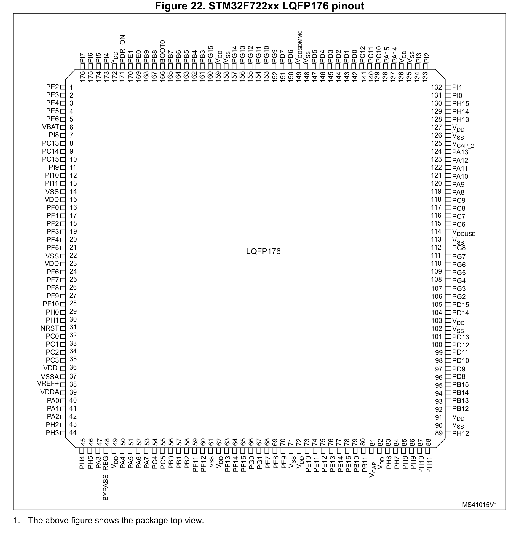
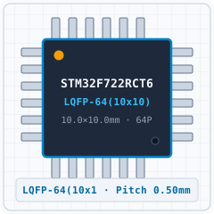
LQFP-64(10x10) · 64P
IPC-7351B
64P10.0×10.0×1.60mmP=0.5mm
STM32F722 / STM32F723 (LQFP-64(10x10))
| Pin | Symbol | Type | Function (EN) |
|---|---|---|---|
| 1 | VBAT | Power | Power Supply Input (VBAT — 3.3V VDD (Max 4.0V)) |
| 2 | PC13 | I/O | Multiplexed I/O & Peripheral Pin PC13 (RTC/CLK) |
| 3 | 3V3 | Power | 3.3V Main Power Supply Rail (3.0V ~ 3.6V) |
| 4 | NC | NC | No Connect (Leave Floating) |
| 5 | PH0OSC IN -_ | I/O | Multiplexed I/O & Peripheral Pin PH0OSC IN -_ (RTC/CLK) |
| 6 | PH1OSC OUT -_ | I/O | Multiplexed I/O & Peripheral Pin PH1OSC OUT -_ (RTC/CLK) |
| 7 | NRST | I | System Enable & Hardware Reset (NRST) |
| 8 | PC0 | I/O | Multiplexed I/O & Peripheral Pin PC0 (ADC) |
| 9 | PC1 | I/O | Multiplexed I/O & Peripheral Pin PC1 (SPI, I2C, ADC, RTC/CLK) |
| 10 | PC2 | I/O | Multiplexed I/O & Peripheral Pin PC2 (SPI, ADC) |
| 11 | PC3 | I/O | Multiplexed I/O & Peripheral Pin PC3 (SPI, ADC) |
| 12 | VSSA | GND | Ground Reference Pin (VSSA) |
| 13 | VREF+ | Analog | Multiplexed I/O & Peripheral Pin VREF+ (General) |
| 14 | PA0WKUP - | I/O | Multiplexed I/O & Peripheral Pin PA0WKUP - (UART, ADC, PWM) |
| 15 | PA1 | I/O | Multiplexed I/O & Peripheral Pin PA1 (UART, ADC, PWM) |
| 16 | PA2 | I/O | Multiplexed I/O & Peripheral Pin PA2 (SPI, ADC, PWM) |
| 17 | PA3 | I/O | Multiplexed I/O & Peripheral Pin PA3 (ADC, PWM) |
| 18 | VSS | GND | Ground Reference Pin (VSS) |
| 19 | VDD | Power | Power Supply Input (VDD — 3.3V VDD (Max 4.0V)) |
| 20 | PA4 | I/O | Multiplexed I/O & Peripheral Pin PA4 (UART, SPI, ADC, DAC) |
| 21 | PA5 | I/O | Multiplexed I/O & Peripheral Pin PA5 (SPI, ADC, DAC, PWM) |
| 22 | PA6 | I/O | Multiplexed I/O & Peripheral Pin PA6 (ADC) |
| 23 | PA7 | I/O | Multiplexed I/O & Peripheral Pin PA7 (SPI, ADC, PWM) |
| 24 | PC4 | I/O | Multiplexed I/O & Peripheral Pin PC4 (ADC) |
| 25 | PB0 | I/O | Multiplexed I/O & Peripheral Pin PB0 (ADC, PWM) |
| 26 | PB1 | I/O | Multiplexed I/O & Peripheral Pin PB1 (ADC, PWM) |
| 27 | PB2 | I/O | Multiplexed I/O & Peripheral Pin PB2 (SPI, I2C) |
| 28 | PB10 | I/O | Multiplexed I/O & Peripheral Pin PB10 (UART, SPI, PWM) |
| 29 | PB11 | I/O | Multiplexed I/O & Peripheral Pin PB11 (UART, PWM) |
| 30 | VCAP_1 | I/O | Multiplexed I/O & Peripheral Pin VCAP_1 (General) |
| 31 | VSS | GND | Ground Reference Pin (VSS) |
| 32 | VDD | Power | Power Supply Input (VDD — 3.3V VDD (Max 4.0V)) |
| 33 | PB12 | I/O | Multiplexed I/O & Peripheral Pin PB12 (UART, SPI) |
| 34 | PB13 | I/O | Multiplexed I/O & Peripheral Pin PB13 (UART, SPI, PWM) |
| 35 | PB14 | I/O | Multiplexed I/O & Peripheral Pin PB14 (SPI, PWM) |
| 36 | PB15 | I/O | Multiplexed I/O & Peripheral Pin PB15 (SPI, PWM, RTC/CLK) |
| 37 | PC6 | I/O | Multiplexed I/O & Peripheral Pin PC6 (PWM) |
| 38 | PC7 | I/O | Multiplexed I/O & Peripheral Pin PC7 (PWM) |
| 39 | PC8 | I/O | Multiplexed I/O & Peripheral Pin PC8 (UART, PWM) |
| 40 | PC9 | I/O | Multiplexed I/O & Peripheral Pin PC9 (UART, I2C, RTC/CLK) |
| 41 | PA8 | I/O | Multiplexed I/O & Peripheral Pin PA8 (I2C, RTC/CLK) |
| 42 | PA9 | I/O | Multiplexed I/O & Peripheral Pin PA9 (UART, SPI, PWM) |
| 43 | PA10 | I/O | Multiplexed I/O & Peripheral Pin PA10 (PWM) |
| 44 | PA11 | I/O | Multiplexed I/O & Peripheral Pin PA11 (PWM, CAN) |
| 45 | PA12 | I/O | Multiplexed I/O & Peripheral Pin PA12 (General) |
| 46 | PA13(JTMS - SWDIO) | I/O | Multiplexed I/O & Peripheral Pin PA13(JTMS - SWDIO) (SWD/JTAG) |
| 47 | VSS | GND | Ground Reference Pin (VSS) |
| 48 | VDD | Power | Power Supply Input (VDD — 3.3V VDD (Max 4.0V)) |
| 49 | PA14(JTCK - SWCLK) | I/O | Multiplexed I/O & Peripheral Pin PA14(JTCK - SWCLK) (SWD/JTAG) |
| 50 | PA15(JTDI) | I/O | Multiplexed I/O & Peripheral Pin PA15(JTDI) (UART, SPI, SWD/JTAG) |
| 51 | PC10 | I/O | Multiplexed I/O & Peripheral Pin PC10 (UART, SPI) |
| 52 | PC11 | I/O | Multiplexed I/O & Peripheral Pin PC11 (UART, SPI) |
| 53 | PC12 | I/O | Multiplexed I/O & Peripheral Pin PC12 (UART, SPI) |
| 54 | PD2 | I/O | Multiplexed I/O & Peripheral Pin PD2 (UART) |
| 55 | PB3(JTDO/TRA CESWO) | I/O | Multiplexed I/O & Peripheral Pin PB3(JTDO/TRA CESWO) (SPI, SWD/JTAG) |
| 56 | PB4(NJTRST) | I/O | Multiplexed I/O & Peripheral Pin PB4(NJTRST) (SPI, SWD/JTAG) |
| 57 | PB5 | I/O | Multiplexed I/O & Peripheral Pin PB5 (SPI, PWM) |
| 58 | PB6 | I/O | Multiplexed I/O & Peripheral Pin PB6 (UART, PWM) |
| 59 | PB7 | I/O | Multiplexed I/O & Peripheral Pin PB7 (UART, PWM) |
| 60 | BOOT | I/O | Multiplexed I/O & Peripheral Pin BOOT (General) |
| 61 | PB8 | I/O | Multiplexed I/O & Peripheral Pin PB8 (I2C, PWM) |
| 62 | PB9 | I/O | Multiplexed I/O & Peripheral Pin PB9 (SPI, I2C, PWM, CAN) |
| 63 | VSS | GND | Ground Reference Pin (VSS) |
| 64 | VDD | Power | Power Supply Input (VDD — 3.3V VDD (Max 4.0V)) |
| 65 | PF15 | I/O | Multiplexed I/O & Peripheral Pin PF15 (General) |
| 66 | PG0 | I/O | Multiplexed I/O & Peripheral Pin PG0 (General) |
| 67 | PG1 | I/O | Multiplexed I/O & Peripheral Pin PG1 (General) |
| 68 | PE7 | I/O | Multiplexed I/O & Peripheral Pin PE7 (General) |
| 69 | PE8 | I/O | Multiplexed I/O & Peripheral Pin PE8 (General) |
| 70 | PE9 | I/O | Multiplexed I/O & Peripheral Pin PE9 (General) |
| 71 | VSS | GND | Ground Reference Pin (VSS) |
| 72 | VDD | Power | Power Supply Input (VDD — 3.3V VDD (Max 4.0V)) |
| 73 | PE10 | I/O | Multiplexed I/O & Peripheral Pin PE10 (General) |
| 74 | PE11 | I/O | Multiplexed I/O & Peripheral Pin PE11 (General) |
| 75 | PE12 | I/O | Multiplexed I/O & Peripheral Pin PE12 (General) |
| 76 | PE13 | I/O | Multiplexed I/O & Peripheral Pin PE13 (General) |
| 77 | PE14 | I/O | Multiplexed I/O & Peripheral Pin PE14 (General) |
| 78 | PE15 | I/O | Multiplexed I/O & Peripheral Pin PE15 (General) |
| 79 | PB10 | I/O | Multiplexed I/O & Peripheral Pin PB10 (General) |
| 80 | PB11 | I/O | Multiplexed I/O & Peripheral Pin PB11 (General) |
| 81 | VCAP_1 | I/O | Multiplexed I/O & Peripheral Pin VCAP_1 (General) |
| 82 | VDD | Power | Power Supply Input (VDD — 3.3V VDD (Max 4.0V)) |
| 83 | PH6 | I/O | Multiplexed I/O & Peripheral Pin PH6 (General) |
| 84 | PH7 | I/O | Multiplexed I/O & Peripheral Pin PH7 (General) |
| 85 | PH8 | I/O | Multiplexed I/O & Peripheral Pin PH8 (General) |
| 86 | PH9 | I/O | Multiplexed I/O & Peripheral Pin PH9 (General) |
| 87 | PH10 | I/O | Multiplexed I/O & Peripheral Pin PH10 (General) |
| 88 | PH11 | I/O | Multiplexed I/O & Peripheral Pin PH11 (General) |
| 89 | PH12 | I/O | Multiplexed I/O & Peripheral Pin PH12 (General) |
| 90 | VSS | GND | Ground Reference Pin (VSS) |
| 91 | VDD | Power | Power Supply Input (VDD — 3.3V VDD (Max 4.0V)) |
| 92 | PB12 | I/O | Multiplexed I/O & Peripheral Pin PB12 (General) |
| 93 | PB13 | I/O | Multiplexed I/O & Peripheral Pin PB13 (General) |
| 94 | PB14 | I/O | Multiplexed I/O & Peripheral Pin PB14 (General) |
| 95 | PB15 | I/O | Multiplexed I/O & Peripheral Pin PB15 (General) |
| 96 | PD8 | I/O | Multiplexed I/O & Peripheral Pin PD8 (General) |
| 97 | PD9 | I/O | Multiplexed I/O & Peripheral Pin PD9 (General) |
| 98 | PD10 | I/O | Multiplexed I/O & Peripheral Pin PD10 (General) |
| 99 | PD11 | I/O | Multiplexed I/O & Peripheral Pin PD11 (General) |
| 100 | PD12 | I/O | Multiplexed I/O & Peripheral Pin PD12 (General) |
| 101 | PD13 | I/O | Multiplexed I/O & Peripheral Pin PD13 (General) |
| 102 | VSS | GND | Ground Reference Pin (VSS) |
| 103 | VDD | Power | Power Supply Input (VDD — 3.3V VDD (Max 4.0V)) |
| 104 | PD14 | I/O | Multiplexed I/O & Peripheral Pin PD14 (General) |
| 105 | PD15 | I/O | Multiplexed I/O & Peripheral Pin PD15 (General) |
| 106 | PG2 | I/O | Multiplexed I/O & Peripheral Pin PG2 (General) |
| 107 | PG3 | I/O | Multiplexed I/O & Peripheral Pin PG3 (General) |
| 108 | PG4 | I/O | Multiplexed I/O & Peripheral Pin PG4 (General) |
| 109 | PG5 | I/O | Multiplexed I/O & Peripheral Pin PG5 (General) |
| 110 | PG6 | I/O | Multiplexed I/O & Peripheral Pin PG6 (General) |
| 111 | PG7 | I/O | Multiplexed I/O & Peripheral Pin PG7 (General) |
| 112 | PG8 | I/O | Multiplexed I/O & Peripheral Pin PG8 (General) |
| 113 | VSS | GND | Ground Reference Pin (VSS) |
| 114 | VDDUSB | Power | Power Supply Input (VDDUSB — 3.3V VDD (Max 4.0V)) |
| 115 | PC6 | I/O | Multiplexed I/O & Peripheral Pin PC6 (General) |
| 116 | PC7 | I/O | Multiplexed I/O & Peripheral Pin PC7 (General) |
| 117 | PC8 | I/O | Multiplexed I/O & Peripheral Pin PC8 (General) |
| 118 | PC9 | I/O | Multiplexed I/O & Peripheral Pin PC9 (General) |
| 119 | PA8 | I/O | Multiplexed I/O & Peripheral Pin PA8 (General) |
| 120 | PA9 | I/O | Multiplexed I/O & Peripheral Pin PA9 (General) |
| 121 | PA10 | I/O | Multiplexed I/O & Peripheral Pin PA10 (General) |
| 122 | PA11 | I/O | Multiplexed I/O & Peripheral Pin PA11 (General) |
| 123 | PA12 | I/O | Multiplexed I/O & Peripheral Pin PA12 (General) |
| 124 | PA13 | I/O | Multiplexed I/O & Peripheral Pin PA13 (General) |
| 125 | PG10 | I/O | Multiplexed I/O & Peripheral Pin PG10 (General) |
| 126 | PG11 | I/O | Multiplexed I/O & Peripheral Pin PG11 (General) |
| 127 | PG12 | I/O | Multiplexed I/O & Peripheral Pin PG12 (General) |
| 128 | PG13 | I/O | Multiplexed I/O & Peripheral Pin PG13 (UART) |
| 129 | PG14 | I/O | Multiplexed I/O & Peripheral Pin PG14 (UART) |
| 130 | VSS | GND | Ground Reference Pin (VSS) |
| 131 | PI0 | I/O | Multiplexed I/O & Peripheral Pin PI0 (General) |
| 132 | PI1 | I/O | Multiplexed I/O & Peripheral Pin PI1 (General) |
| 133 | PI2 | I/O | Multiplexed I/O & Peripheral Pin PI2 (General) |
| 134 | PI3 | I/O | Multiplexed I/O & Peripheral Pin PI3 (General) |
| 135 | VSS | GND | Ground Reference Pin (VSS) |
| 136 | VDD | Power | Power Supply Input (VDD — 3.3V VDD (Max 4.0V)) |
| 137 | PA14 | I/O | Multiplexed I/O & Peripheral Pin PA14 (General) |
| 138 | PA15 | I/O | Multiplexed I/O & Peripheral Pin PA15 (General) |
| 139 | PC10 | I/O | Multiplexed I/O & Peripheral Pin PC10 (General) |
| 140 | PC11 | I/O | Multiplexed I/O & Peripheral Pin PC11 (General) |
| 141 | PC12 | I/O | Multiplexed I/O & Peripheral Pin PC12 (General) |
| 142 | PD0 | I/O | Multiplexed I/O & Peripheral Pin PD0 (General) |
| 143 | PD1 | I/O | Multiplexed I/O & Peripheral Pin PD1 (General) |
| 144 | PD2 | I/O | Multiplexed I/O & Peripheral Pin PD2 (General) |
| 145 | PD3 | I/O | Multiplexed I/O & Peripheral Pin PD3 (General) |
| 146 | PD4 | I/O | Multiplexed I/O & Peripheral Pin PD4 (General) |
| 147 | PD5 | I/O | Multiplexed I/O & Peripheral Pin PD5 (General) |
| 148 | VSS | GND | Ground Reference Pin (VSS) |
| 149 | VDDSDMMC | Power | Power Supply Input (VDDSDMMC — 3.3V VDD (Max 4.0V)) |
| 150 | PD6 | I/O | Multiplexed I/O & Peripheral Pin PD6 (General) |
| 151 | PD7 | I/O | Multiplexed I/O & Peripheral Pin PD7 (General) |
| 152 | PG9 | I/O | Multiplexed I/O & Peripheral Pin PG9 (General) |
| 153 | PG10 | I/O | Multiplexed I/O & Peripheral Pin PG10 (General) |
| 154 | PG11 | I/O | Multiplexed I/O & Peripheral Pin PG11 (General) |
| 155 | PG12 | I/O | Multiplexed I/O & Peripheral Pin PG12 (General) |
| 156 | PG13 | I/O | Multiplexed I/O & Peripheral Pin PG13 (General) |
| 157 | PG14 | I/O | Multiplexed I/O & Peripheral Pin PG14 (General) |
| 158 | VSS | GND | Ground Reference Pin (VSS) |
| 159 | VDD | Power | Power Supply Input (VDD — 3.3V VDD (Max 4.0V)) |
| 160 | PG15 | I/O | Multiplexed I/O & Peripheral Pin PG15 (General) |
| 161 | PB3 | I/O | Multiplexed I/O & Peripheral Pin PB3 (General) |
| 162 | PB4 | I/O | Multiplexed I/O & Peripheral Pin PB4 (General) |
| 163 | PB5 | I/O | Multiplexed I/O & Peripheral Pin PB5 (General) |
| 164 | PB6 | I/O | Multiplexed I/O & Peripheral Pin PB6 (General) |
| 165 | PB7 | I/O | Multiplexed I/O & Peripheral Pin PB7 (General) |
| 166 | BOOT0 | I | Input-Only Pin BOOT0 (General) |
| 167 | PB8 | I/O | Multiplexed I/O & Peripheral Pin PB8 (General) |
| 168 | PB9 | I/O | Multiplexed I/O & Peripheral Pin PB9 (General) |
| 169 | PE0 | I/O | Multiplexed I/O & Peripheral Pin PE0 (General) |
| 170 | PE1 | I/O | Multiplexed I/O & Peripheral Pin PE1 (General) |
| 171 | PDR_ON | I/O | Multiplexed I/O & Peripheral Pin PDR_ON (General) |
| 172 | VDD | Power | Power Supply Input (VDD — 3.3V VDD (Max 4.0V)) |
| 173 | PI4 | I/O | Multiplexed I/O & Peripheral Pin PI4 (General) |
| 174 | PI5 | I/O | Multiplexed I/O & Peripheral Pin PI5 (General) |
| 175 | PI6 | I/O | Multiplexed I/O & Peripheral Pin PI6 (General) |
| 176 | PI7 | I/O | Multiplexed I/O & Peripheral Pin PI7 (General) |
STM32F722 / STM32F723 (LQFP-64(10x10))
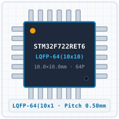
STM32F722 / STM32F723 (LQFP-64(10x10))
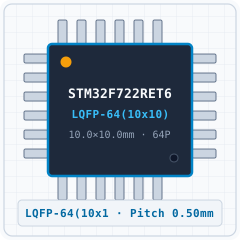
STM32F722 / STM32F723 (LQFP-64(10x10))
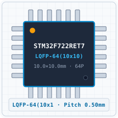
STM32F722 / STM32F723 (LQFP-64(10x10))
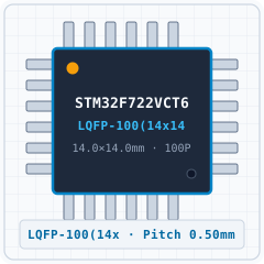
STM32F722 / STM32F723 (LQFP-100(14x14))
STM32F722 / STM32F723 (LQFP-100(14x14))
STM32F722 / STM32F723 (LQFP-100(14x14))
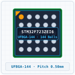
STM32F722 / STM32F723 (LQFP-144(20x20))
STM32F722 / STM32F723 (LQFP-144(20x20))
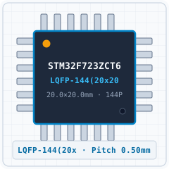
STM32F722 / STM32F723 (LQFP-144(20x20))

STM32F722 / STM32F723 (LQFP-144(20x20))
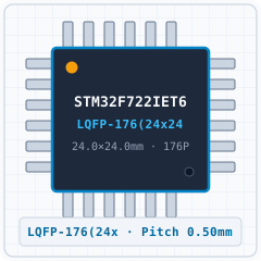
STM32F722 / STM32F723 (LQFP-176(24x24))
STM32F722 / STM32F723 (LQFP-176(24x24))
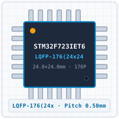
STM32F722 / STM32F723 (LQFP-176(24x24))
| Designator / Replacement MPN | Value / Package | Function & PCB Layout Rule |
|---|---|---|
| N/A BOM | Per application circuit LQFP-176(24x24) | Size power & signal trace widths for rated load current following IPC-2221 clearance rules. |
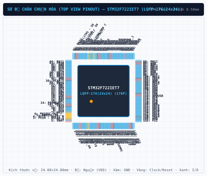
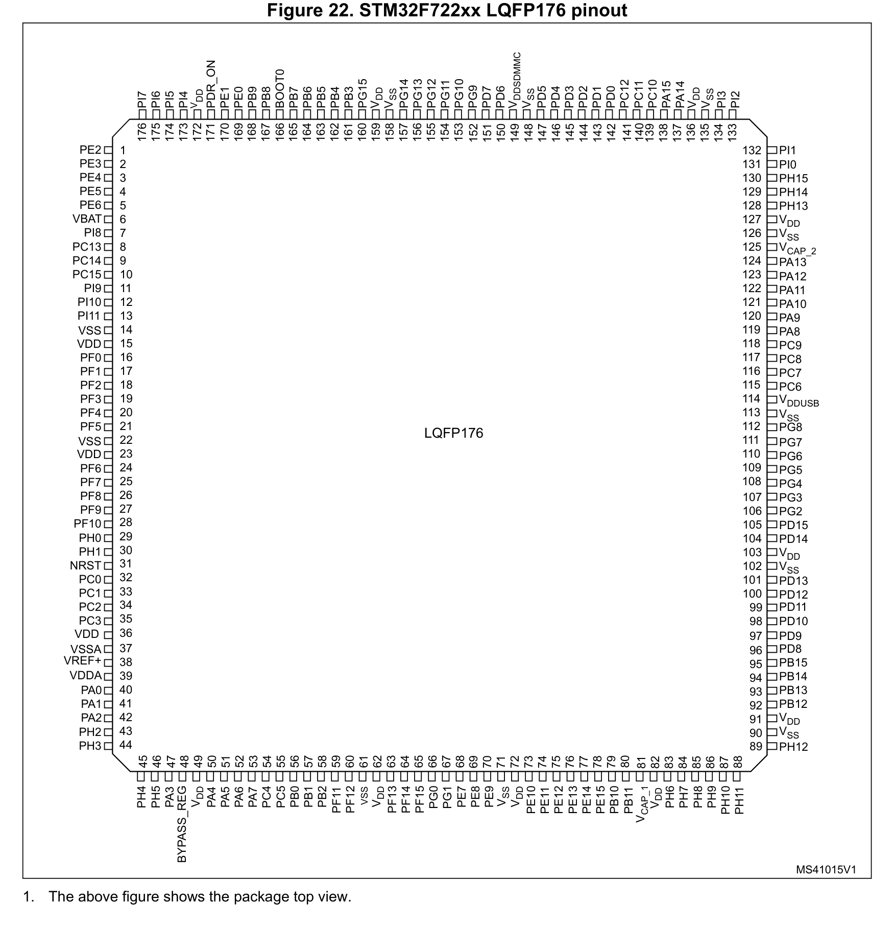
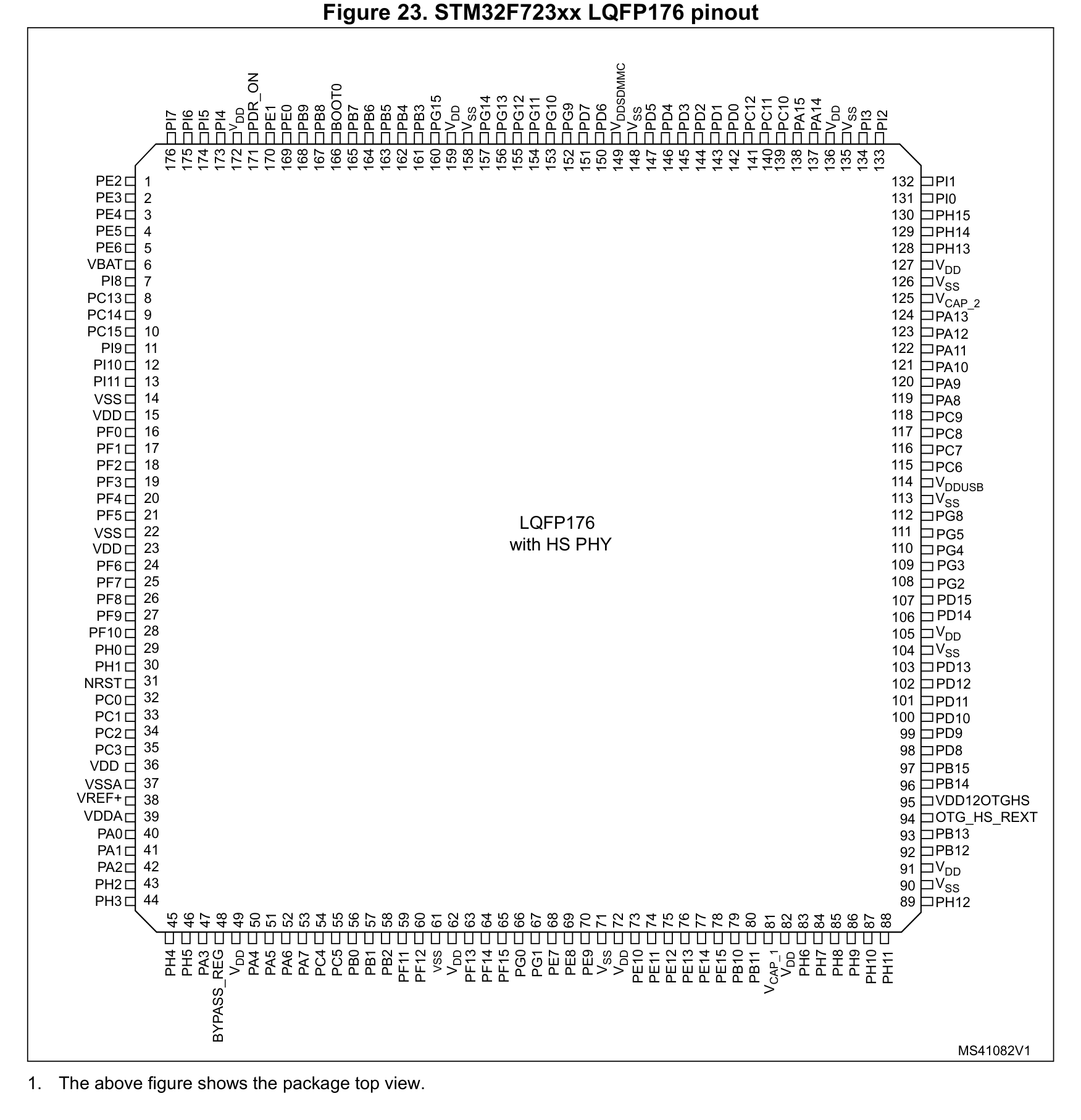
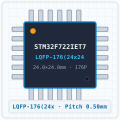
Manufactured by ST, the STM32F722IET7 is housed in a LQFP-176(24x24) package with 176 pins and a 0.50 mm lead pitch, supporting a VCC supply range of 1.7 V to 3.6 V. Key pins include: 1 (VBAT: Power Supply Input (VBAT — 3.3V VDD (Max 4.0V))), 2 (PC13: Multiplexed I/O & Peripheral Pin PC13 (RTC/CLK)), 3 (3V3: 3.3V Main Power Supply Rail (3.0V ~ 3.6V)), 4 (NC: No Connect (Leave Floating)), 5 (PH0OSC IN -_: Multiplexed I/O & Peripheral Pin PH0OSC IN -_ (RTC/CLK)), 6 (PH1OSC OUT -_: Multiplexed I/O & Peripheral Pin PH1OSC OUT -_ (RTC/CLK)).
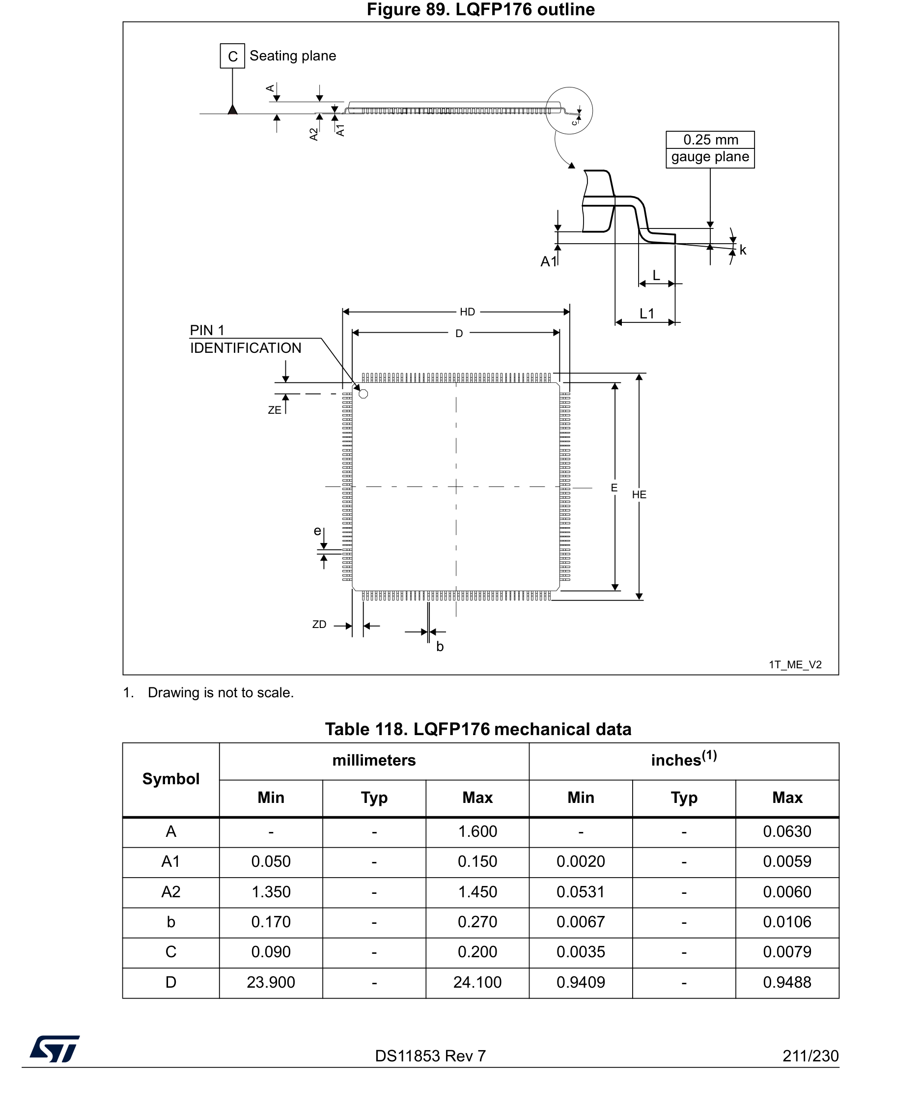
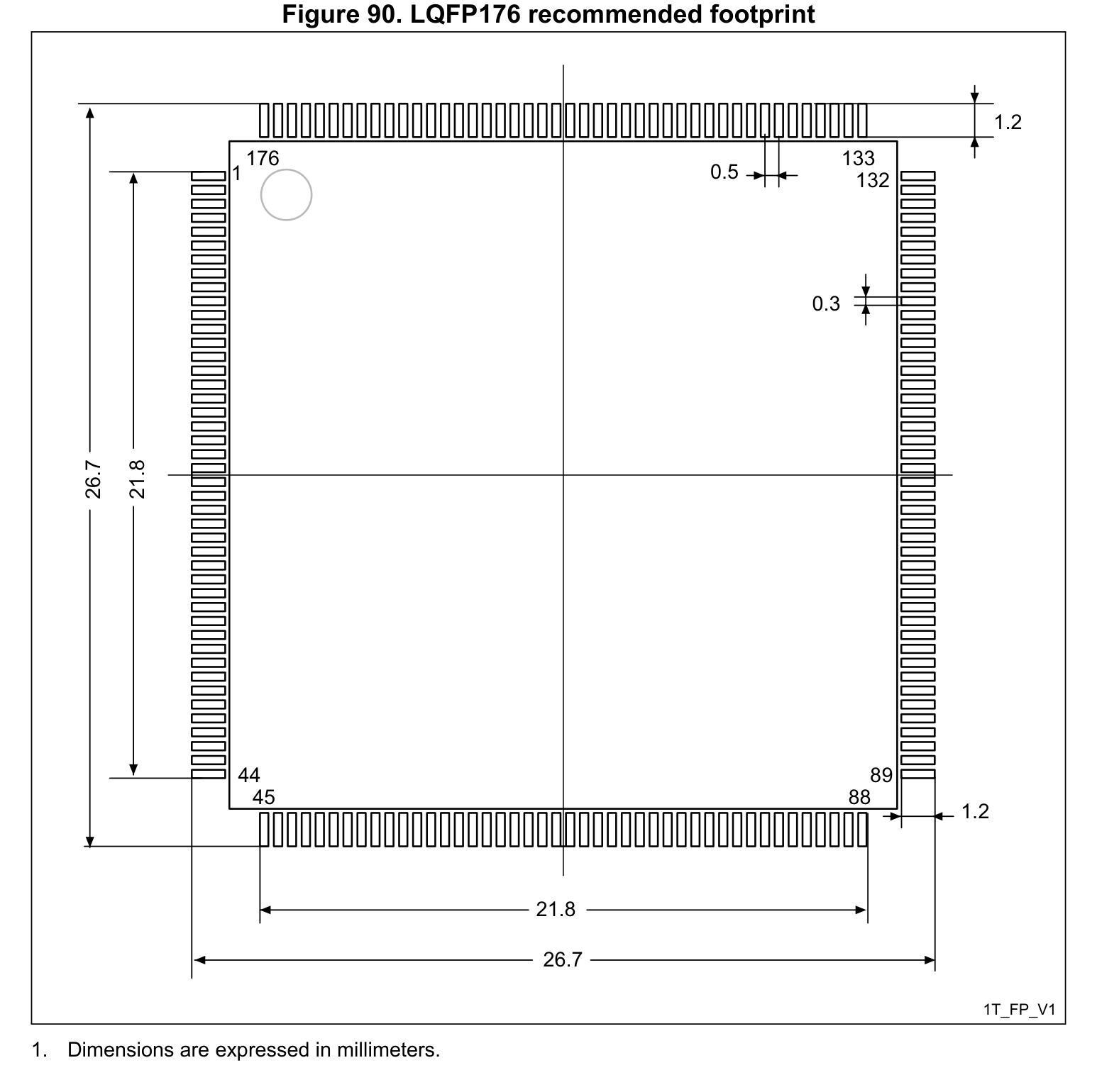
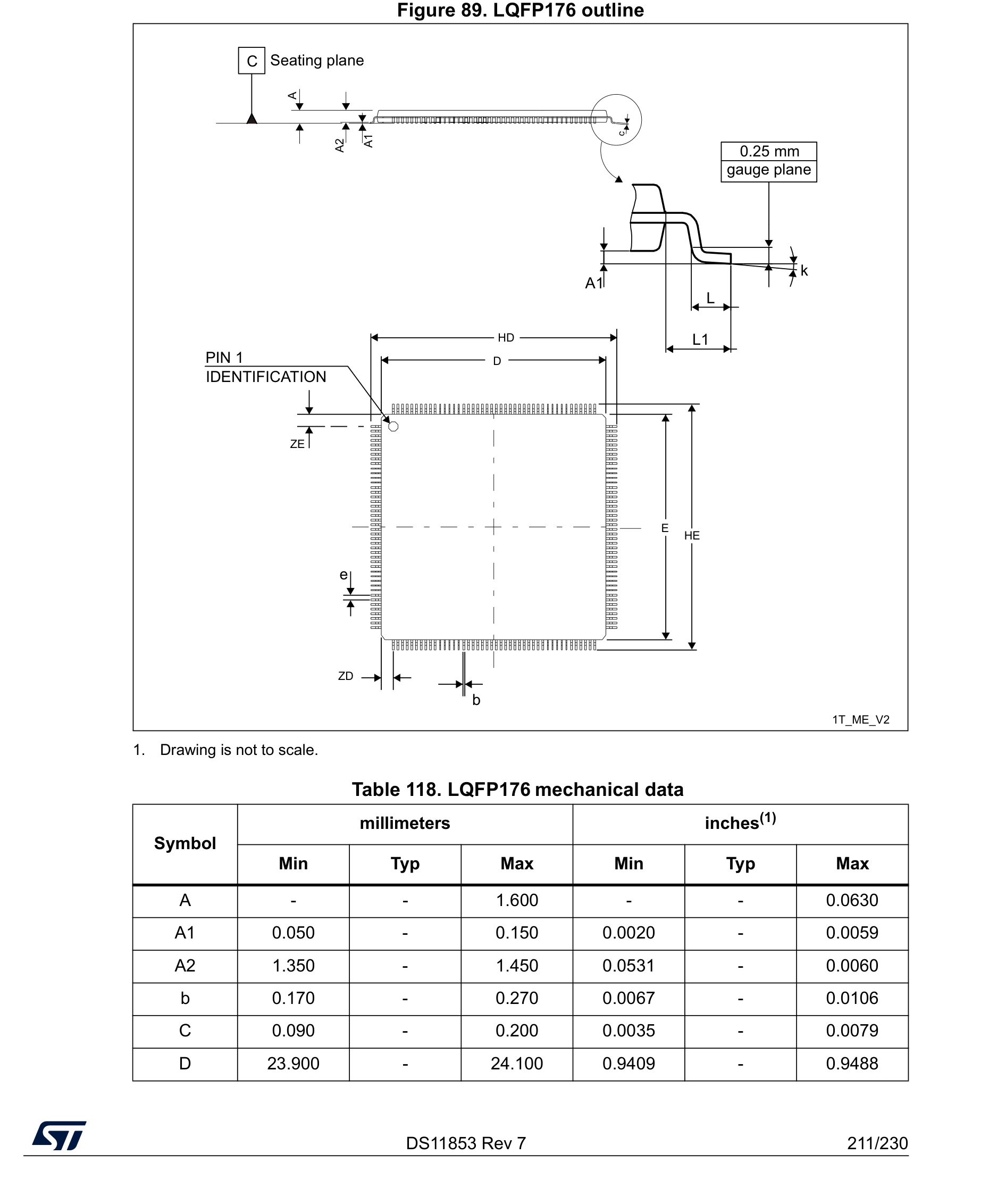
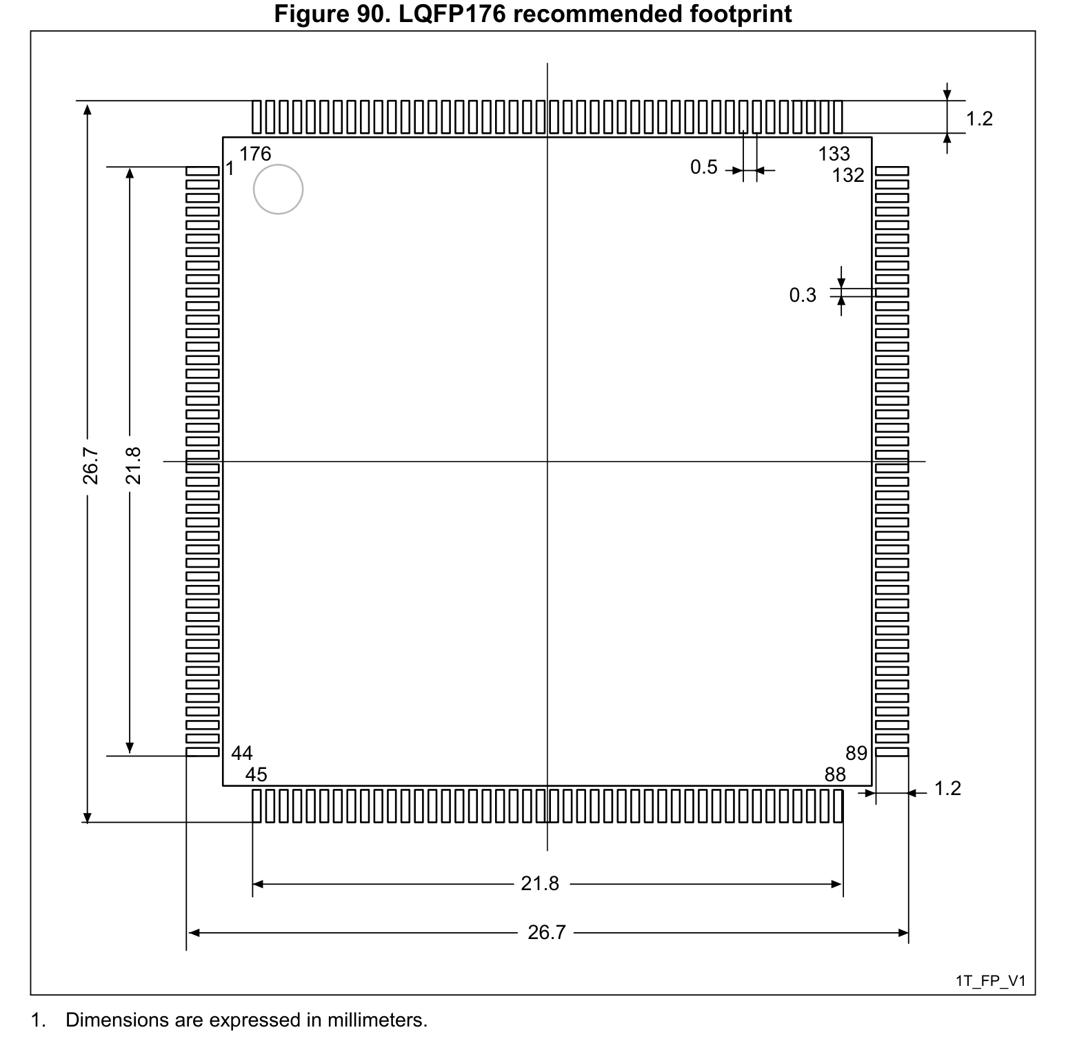
Normalized from the official datasheet mechanical drawing per IPC-7351B (Density Level B Nominal), STM32F722IET7 (LQFP-176(24x24)) has a nominal body envelope of 24.00 × 24.00 mm, pitch e = 0.50 mm, and 176 copper pads.
You can download the verified open-hardware (CERN-OHL-P-2.0) CAD library bundle for STM32F722IET7 (ST, LQFP-176(24x24)) directly on this page, including KiCad 8 Footprints (.kicad_mod), Schematic Symbols (.kicad_sym), Autodesk Fusion 360 / Eagle (.lbr), and 3D STEP AP214 / WebGL GLB models.
| Pin # | Signal Name | Electrical Type | Functional Description & Design Notes |
|---|---|---|---|
| 1 | VBAT | Power_In | Primary positive power supply input (VBAT) operating in the 3.3V VDD (Max 4.0V) domain (Max rating: 4.0V). |
| 2 | PC13 | Digital_IO | Signal terminal PC13 (I/O, 3.3V VDD (5V-Tolerant FT) domain). Multiplexed alternate functions: PC13. Supported peripheral buses: RTC/CLK. |
| 3 | 3V3 | Power_In | 3.3V Main Power Supply Rail (3.0V ~ 3.6V) |
| 4 | NC | No_Connect | No Connect (Leave Floating) |
| 5 | PH0OSC IN -_ | Digital_IO | Signal terminal PH0OSC IN -_ (I/O, 3.3V VDD (5V-Tolerant FT) domain). Multiplexed alternate functions: PH0OSC IN -_. Supported peripheral buses: RTC/CLK. |
| 6 | PH1OSC OUT -_ | Digital_IO | Signal terminal PH1OSC OUT -_ (I/O, 3.3V VDD (5V-Tolerant FT) domain). Multiplexed alternate functions: PH1OSC OUT -_. Supported peripheral buses: RTC/CLK. |
| 7 | NRST | Digital_IO | Active-low hardware reset terminal (NRST): pulling this pin Low resets the processor core and peripherals. |
| 8 | PC0 | Digital_IO | Signal terminal PC0 (I/O, 3.3V VDD (5V-Tolerant FT) domain). Multiplexed alternate functions: PC0. Supported peripheral buses: ADC. |
| 9 | PC1 | Digital_IO | Signal terminal PC1 (I/O, 3.3V VDD (5V-Tolerant FT) domain). Multiplexed alternate functions: SPI2_MOSI. Supported peripheral buses: SPI, I2C, ADC, RTC/CLK. |
| 10 | PC2 | Digital_IO | Signal terminal PC2 (I/O, 3.3V VDD (5V-Tolerant FT) domain). Multiplexed alternate functions: SPI2_MISO. Supported peripheral buses: SPI, ADC. |
| 11 | PC3 | Digital_IO | Signal terminal PC3 (I/O, 3.3V VDD (5V-Tolerant FT) domain). Multiplexed alternate functions: SPI2_MOSI. Supported peripheral buses: SPI, ADC. |
| 12 | VSSA | GND | 0V electrical ground return terminal (VSSA) for internal core logic, I/O drivers, and analog sub-blocks. |
| 13 | VREF+ | Analog | Signal terminal VREF+ (Analog, 3.3V VDD (Max 4.0V) domain). Multiplexed alternate functions: VREF+. Supported peripheral buses: General. |
| 14 | PA0WKUP - | Digital_IO | Signal terminal PA0WKUP - (I/O, 3.3V VDD (5V-Tolerant FT) domain). Multiplexed alternate functions: PA0WKUP -. Supported peripheral buses: UART, ADC, PWM. |
| 15 | PA1 | Digital_IO | Signal terminal PA1 (I/O, 3.3V VDD (5V-Tolerant FT) domain). Multiplexed alternate functions: PA1. Supported peripheral buses: UART, ADC, PWM. |
| 16 | PA2 | Digital_IO | Signal terminal PA2 (I/O, 3.3V VDD (5V-Tolerant FT) domain). Multiplexed alternate functions: PA2. Supported peripheral buses: SPI, ADC, PWM. |
| 17 | PA3 | Digital_IO | Signal terminal PA3 (I/O, 3.3V VDD (5V-Tolerant FT) domain). Multiplexed alternate functions: PA3. Supported peripheral buses: ADC, PWM. |
| 18 | VSS | GND | 0V electrical ground return terminal (VSS) for internal core logic, I/O drivers, and analog sub-blocks. |
| 19 | VDD | Power_In | Primary positive power supply input (VDD) operating in the 3.3V VDD (Max 4.0V) domain (Max rating: 4.0V). |
| 20 | PA4 | Digital_IO | Signal terminal PA4 (I/O, 3.3V VDD (Max 4.0V) domain). Multiplexed alternate functions: SPI1_NSS, SPI3_NSS. Supported peripheral buses: UART, SPI, ADC, DAC. |
| 21 | PA5 | Digital_IO | Signal terminal PA5 (I/O, 3.3V VDD (Max 4.0V) domain). Multiplexed alternate functions: SPI1_SCK. Supported peripheral buses: SPI, ADC, DAC, PWM. |
| 22 | PA6 | Digital_IO | Signal terminal PA6 (I/O, 3.3V VDD (5V-Tolerant FT) domain). Multiplexed alternate functions: PA6. Supported peripheral buses: ADC. |
| 23 | PA7 | Digital_IO | Signal terminal PA7 (I/O, 3.3V VDD (5V-Tolerant FT) domain). Multiplexed alternate functions: SPI1_MOSI. Supported peripheral buses: SPI, ADC, PWM. |
| 24 | PC4 | Digital_IO | Signal terminal PC4 (I/O, 3.3V VDD (5V-Tolerant FT) domain). Multiplexed alternate functions: PC4. Supported peripheral buses: ADC. |
| 25 | PB0 | Digital_IO | Signal terminal PB0 (I/O, 3.3V VDD (5V-Tolerant FT) domain). Multiplexed alternate functions: PB0. Supported peripheral buses: ADC, PWM. |
| 26 | PB1 | Digital_IO | Signal terminal PB1 (I/O, 3.3V VDD (5V-Tolerant FT) domain). Multiplexed alternate functions: PB1. Supported peripheral buses: ADC, PWM. |
| 27 | PB2 | Digital_IO | Signal terminal PB2 (I/O, 3.3V VDD (5V-Tolerant FT) domain). Multiplexed alternate functions: SPI3_MOSI. Supported peripheral buses: SPI, I2C. |
| 28 | PB10 | Digital_IO | Signal terminal PB10 (I/O, 3.3V VDD (5V-Tolerant FT) domain). Multiplexed alternate functions: SPI2_SCK. Supported peripheral buses: UART, SPI, PWM. |
| 29 | PB11 | Digital_IO | Signal terminal PB11 (I/O, 3.3V VDD (5V-Tolerant FT) domain). Multiplexed alternate functions: PB11. Supported peripheral buses: UART, PWM. |
| 30 | VCAP_1 | Digital_IO | Signal terminal VCAP_1 (I/O, 3.3V VDD (Max 4.0V) domain). Multiplexed alternate functions: VCAP_1. Supported peripheral buses: General. |
| 31 | VSS | GND | 0V electrical ground return terminal (VSS) for internal core logic, I/O drivers, and analog sub-blocks. |
| 32 | VDD | Power_In | Primary positive power supply input (VDD) operating in the 3.3V VDD (Max 4.0V) domain (Max rating: 4.0V). |
| 33 | PB12 | Digital_IO | Signal terminal PB12 (I/O, 3.3V VDD (5V-Tolerant FT) domain). Multiplexed alternate functions: SPI2_NSS. Supported peripheral buses: UART, SPI. |
| 34 | PB13 | Digital_IO | Signal terminal PB13 (I/O, 3.3V VDD (5V-Tolerant FT) domain). Multiplexed alternate functions: SPI2_SCK. Supported peripheral buses: UART, SPI, PWM. |
| 35 | PB14 | Digital_IO | Signal terminal PB14 (I/O, 3.3V VDD (5V-Tolerant FT) domain). Multiplexed alternate functions: SPI2_MISOUSART3RTS. Supported peripheral buses: SPI, PWM. |
| 36 | PB15 | Digital_IO | Signal terminal PB15 (I/O, 3.3V VDD (5V-Tolerant FT) domain). Multiplexed alternate functions: SPI2_MOSI. Supported peripheral buses: SPI, PWM, RTC/CLK. |
| 37 | PC6 | Digital_IO | Signal terminal PC6 (I/O, 3.3V VDD (5V-Tolerant FT) domain). Multiplexed alternate functions: PC6. Supported peripheral buses: PWM. |
| 38 | PC7 | Digital_IO | Signal terminal PC7 (I/O, 3.3V VDD (5V-Tolerant FT) domain). Multiplexed alternate functions: PC7. Supported peripheral buses: PWM. |
| 39 | PC8 | Digital_IO | Signal terminal PC8 (I/O, 3.3V VDD (5V-Tolerant FT) domain). Multiplexed alternate functions: PC8. Supported peripheral buses: UART, PWM. |
| 40 | PC9 | Digital_IO | Signal terminal PC9 (I/O, 3.3V VDD (5V-Tolerant FT) domain). Multiplexed alternate functions: PC9. Supported peripheral buses: UART, I2C, RTC/CLK. |
| 41 | PA8 | Digital_IO | Signal terminal PA8 (I/O, 3.3V VDD (5V-Tolerant FT) domain). Multiplexed alternate functions: PA8. Supported peripheral buses: I2C, RTC/CLK. |
| 42 | PA9 | Digital_IO | Signal terminal PA9 (I/O, 3.3V VDD (5V-Tolerant FT) domain). Multiplexed alternate functions: SPI2_SCK. Supported peripheral buses: UART, SPI, PWM. |
| 43 | PA10 | Digital_IO | Signal terminal PA10 (I/O, 3.3V VDD (5V-Tolerant FT) domain). Multiplexed alternate functions: PA10. Supported peripheral buses: PWM. |
| 44 | PA11 | Digital_IO | Signal terminal PA11 (I/O, 3.3V VDD (5V-Tolerant FT) domain). Multiplexed alternate functions: PA11. Supported peripheral buses: PWM, CAN. |
| 45 | PA12 | Digital_IO | Signal terminal PA12 (I/O, 3.3V VDD (5V-Tolerant FT) domain). Multiplexed alternate functions: PA12. Supported peripheral buses: General. |
| 46 | PA13(JTMS - SWDIO) | Digital_IO | Signal terminal PA13(JTMS - SWDIO) (I/O, 3.3V VDD (5V-Tolerant FT) domain). Multiplexed alternate functions: PA13(JTMS - SWDIO). Supported peripheral buses: SWD/JTAG. |
| 47 | VSS | GND | 0V electrical ground return terminal (VSS) for internal core logic, I/O drivers, and analog sub-blocks. |
| 48 | VDD | Power_In | Primary positive power supply input (VDD) operating in the 3.3V VDD (Max 4.0V) domain (Max rating: 4.0V). |
| 49 | PA14(JTCK - SWCLK) | Digital_IO | Signal terminal PA14(JTCK - SWCLK) (I/O, 3.3V VDD (5V-Tolerant FT) domain). Multiplexed alternate functions: PA14(JTCK - SWCLK). Supported peripheral buses: SWD/JTAG. |
| 50 | PA15(JTDI) | Digital_IO | Signal terminal PA15(JTDI) (I/O, 3.3V VDD (5V-Tolerant FT) domain). Multiplexed alternate functions: SPI1_NSS, SPI3_NSS. Supported peripheral buses: UART, SPI, SWD/JTAG. |
| 51 | PC10 | Digital_IO | Signal terminal PC10 (I/O, 3.3V VDD (5V-Tolerant FT) domain). Multiplexed alternate functions: SPI3_SCK. Supported peripheral buses: UART, SPI. |
| 52 | PC11 | Digital_IO | Signal terminal PC11 (I/O, 3.3V VDD (5V-Tolerant FT) domain). Multiplexed alternate functions: SPI3_MISOUSART3RX. Supported peripheral buses: UART, SPI. |
| 53 | PC12 | Digital_IO | Signal terminal PC12 (I/O, 3.3V VDD (5V-Tolerant FT) domain). Multiplexed alternate functions: SPI3_MOSI. Supported peripheral buses: UART, SPI. |
| 54 | PD2 | Digital_IO | Signal terminal PD2 (I/O, 3.3V VDD (5V-Tolerant FT) domain). Multiplexed alternate functions: PD2. Supported peripheral buses: UART. |
| 55 | PB3(JTDO/TRA CESWO) | Digital_IO | Signal terminal PB3(JTDO/TRA CESWO) (I/O, 3.3V VDD (5V-Tolerant FT) domain). Multiplexed alternate functions: SPI1_SCK, SPI3_SCK. Supported peripheral buses: SPI, SWD/JTAG. |
| 56 | PB4(NJTRST) | Digital_IO | Signal terminal PB4(NJTRST) (I/O, 3.3V VDD (5V-Tolerant FT) domain). Multiplexed alternate functions: SPI1_MISOSPI3MISO, SPI2_NSS. Supported peripheral buses: SPI, SWD/JTAG. |
| 57 | PB5 | Digital_IO | Signal terminal PB5 (I/O, 3.3V VDD (5V-Tolerant FT) domain). Multiplexed alternate functions: SPI1_MOSI, SPI3_MOSI. Supported peripheral buses: SPI, PWM. |
| 58 | PB6 | Digital_IO | Signal terminal PB6 (I/O, 3.3V VDD (5V-Tolerant FT) domain). Multiplexed alternate functions: PB6. Supported peripheral buses: UART, PWM. |
| 59 | PB7 | Digital_IO | Signal terminal PB7 (I/O, 3.3V VDD (5V-Tolerant FT) domain). Multiplexed alternate functions: PB7. Supported peripheral buses: UART, PWM. |
| 60 | BOOT | Digital_IO | Signal terminal BOOT (I/O, 3.3V VDD (Max 4.0V) domain). Multiplexed alternate functions: BOOT. Supported peripheral buses: General. |
| 61 | PB8 | Digital_IO | Signal terminal PB8 (I/O, 3.3V VDD (5V-Tolerant FT) domain). Multiplexed alternate functions: PB8. Supported peripheral buses: I2C, PWM. |
| 62 | PB9 | Digital_IO | Signal terminal PB9 (I/O, 3.3V VDD (5V-Tolerant FT) domain). Multiplexed alternate functions: I2C1_SDA, SPI2_NSS. Supported peripheral buses: SPI, I2C, PWM, CAN. |
| 63 | VSS | GND | 0V electrical ground return terminal (VSS) for internal core logic, I/O drivers, and analog sub-blocks. |
| 64 | VDD | Power_In | Primary positive power supply input (VDD) operating in the 3.3V VDD (Max 4.0V) domain (Max rating: 4.0V). |