
MCP19215T-E/S8 (QFN-32-EP(5x5)) — Symbol, Footprint IPC-7351B & 3D STEP Model

MCP19215T-E/S8

MICROCHIPID: C219057QFN-32-EP(5x5) · 33 Pins · Pitch 0.50mmIPC-7351B Verified5.0 (0)
SYNCHRONIZED 4D CROSS-PROBE MODETouch or hover any pin to highlight concurrently across Symbol, Footprint and 3D
1. SYMBOL
U1 · MCP19215T-E/S8 (QFN-32-EP(5x5))1GPA0/AN0/TS_2GPA1/AN13GPA2/AN2/T0C4GPB4/AN5/ICS5GPA3/AN3/TS_6GPA7/SCL7GPB0/SDA8GPA5/MCLR9GPB7/CCD210GPA6/CCD111AGND/DGND12ISN213ISP214CCOMP215VCOMP216VFB217IP233EPAD32GPB5/AN6/ICS31GPB1/AN4/RX/30GPB6/AN7/TX/29ISN128ISP127CCOMP126VCOMP125VFB124IP123VIN22VDD21VDR20PDRV119PGND18PDRV2Grid Pitch = 2.54mm (IEEE-315)-17.8-12.7-7.6-2.52.57.612.717.827.922.917.812.77.62.5-2.5-7.6-12.7-17.8-22.9-27.9mm
2. 2D FOOTPRINT
123456789101112131415161718192021222324252627282930313233E=5.00mm · Pitch e=0.50mmD=5.00mm-5-4-3-2-1012345543210-1-2-3-4-5mm
3. 3D CAD MODEL
Package Body: 5.00mm × 5.00mm · Pitch: 0.50mm · Ruler Step: 1.00mmSynced <100ms

Synchronized Pinout (Symbol / 2D / 3D) (33/33)

Touch or hover any pin to highlight concurrently across Symbol, Footprint and 3D
PinSymbolTypeFunction (EN)
1GPA0/AN0/TS_OUT1I/OMultiplexed I/O & Peripheral Pin GPA0/AN0/TS_OUT1 (General)
2GPA1/AN1I/OMultiplexed I/O & Peripheral Pin GPA1/AN1 (General)
3GPA2/AN2/T0CKI/INTI/OMultiplexed I/O & Peripheral Pin GPA2/AN2/T0CKI/INT (General)
4GPB4/AN5/ICSPDATI/OMultiplexed I/O & Peripheral Pin GPB4/AN5/ICSPDAT (General)
5GPA3/AN3/TS_OUT2I/OMultiplexed I/O & Peripheral Pin GPA3/AN3/TS_OUT2 (General)
6GPA7/SCLI/OMultiplexed I/O & Peripheral Pin GPA7/SCL (I2C)
7GPB0/SDAI/OMultiplexed I/O & Peripheral Pin GPB0/SDA (I2C)
8GPA5/MCLRI/OMultiplexed I/O & Peripheral Pin GPA5/MCLR (General)
9GPB7/CCD2I/OMultiplexed I/O & Peripheral Pin GPB7/CCD2 (General)
10GPA6/CCD1I/OMultiplexed I/O & Peripheral Pin GPA6/CCD1 (General)
11AGND/DGNDGNDGround Reference Pin (AGND/DGND)
12ISN2I/OMultiplexed I/O & Peripheral Pin ISN2 (General)
13ISP2I/OMultiplexed I/O & Peripheral Pin ISP2 (General)
14CCOMP2I/OMultiplexed I/O & Peripheral Pin CCOMP2 (General)
15VCOMP2I/OMultiplexed I/O & Peripheral Pin VCOMP2 (General)
16VFB2I/OMultiplexed I/O & Peripheral Pin VFB2 (General)
17IP2I/OMultiplexed I/O & Peripheral Pin IP2 (General)
18PDRV2I/OMultiplexed I/O & Peripheral Pin PDRV2 (General)
19PGNDGNDGround Reference Pin (PGND)
20PDRV1I/OMultiplexed I/O & Peripheral Pin PDRV1 (General)
21VDRI/OMultiplexed I/O & Peripheral Pin VDR (General)
22VDDPowerPower Supply Input (VDD — 4.5V-42V)
23VINPowerPower Supply Input (VIN — 4.5V-42V)
24IP1I/OMultiplexed I/O & Peripheral Pin IP1 (General)
25VFB1I/OMultiplexed I/O & Peripheral Pin VFB1 (General)
26VCOMP1I/OMultiplexed I/O & Peripheral Pin VCOMP1 (General)
27CCOMP1I/OMultiplexed I/O & Peripheral Pin CCOMP1 (General)
28ISP1I/OMultiplexed I/O & Peripheral Pin ISP1 (General)
29ISN1I/OMultiplexed I/O & Peripheral Pin ISN1 (General)
30GPB6/AN7/TX/CKI/OMultiplexed I/O & Peripheral Pin GPB6/AN7/TX/CK (General)
31GPB1/AN4/RX/DTI/OMultiplexed I/O & Peripheral Pin GPB1/AN4/RX/DT (General)
32GPB5/AN6/ICSPCLKI/OMultiplexed I/O & Peripheral Pin GPB5/AN6/ICSPCLK (General)
33EPADGNDExposed Thermal & Ground Pad (EPAD)
PIN 1 GPA0/AN0/TS_OUT1
I/O
Multiplexed I/O & Peripheral Pin GPA0/AN0/TS_OUT1 (General)
Design note: Signal terminal GPA0/AN0/TS_OUT1 (I/O, 4.5V-42V domain). Multiplexed alternate functions: GPA0/AN0/TS_OUT1. Supported peripheral buses: General.
IPC-7351B Solder Density & Span C/G/Z Tuner

Live Embedded Datasheet PDF & Technical Drawing Gallery (6 Standard Drawings + 21 Extracted Figures)

Read the original datasheet PDF directly or click any drawing to view fullscreen
Open PDF in New Window ↗Read Datasheet PDF (.pdf)
PDF VIEWEROfficial Datasheet Document: MCP19215T-E/S8 (MICROCHIP · QFN-32-EP(5x5))
Scroll, search text (Ctrl+F), or expand directly inside the embedded PDF reader below
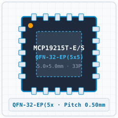
1. Realistic 3D PackageREPRESENTATIVE
MCP19215T-E/S8 (QFN-32-EP(5x5)) - 1. Realistic 3D Package
Detailed solid 3D bodyExpand ›
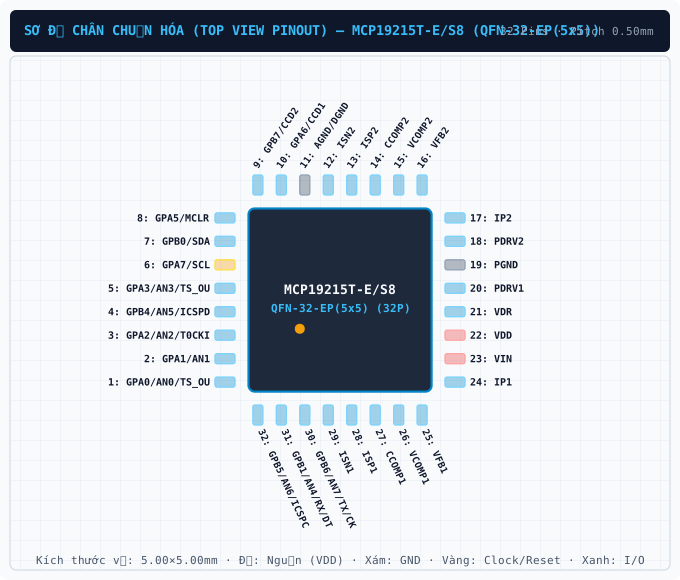
2. Standard Pinout (Top View)CLEANROOM PINOUT
MCP19215T-E/S8 (QFN-32-EP(5x5)) - 2. Standard Pinout (Top View)
True package pinout (33 pins)Expand ›
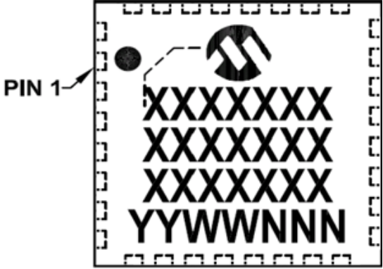
3. Original Datasheet PinoutPDF PINOUT
MCP19215T-E/S8 (QFN-32-EP(5x5)) - 3. Original Datasheet Pinout
Uncropped datasheet pin diagramExpand ›
4. Package Dimensions (D×E×A)PACKAGE DIMENSIONS
MCP19215T-E/S8 (QFN-32-EP(5x5)) - 4. Package Dimensions (D×E×A)
QFN-32-EP(5x5) · 5.00×5.00mm · Pitch 0.50mmExpand ›
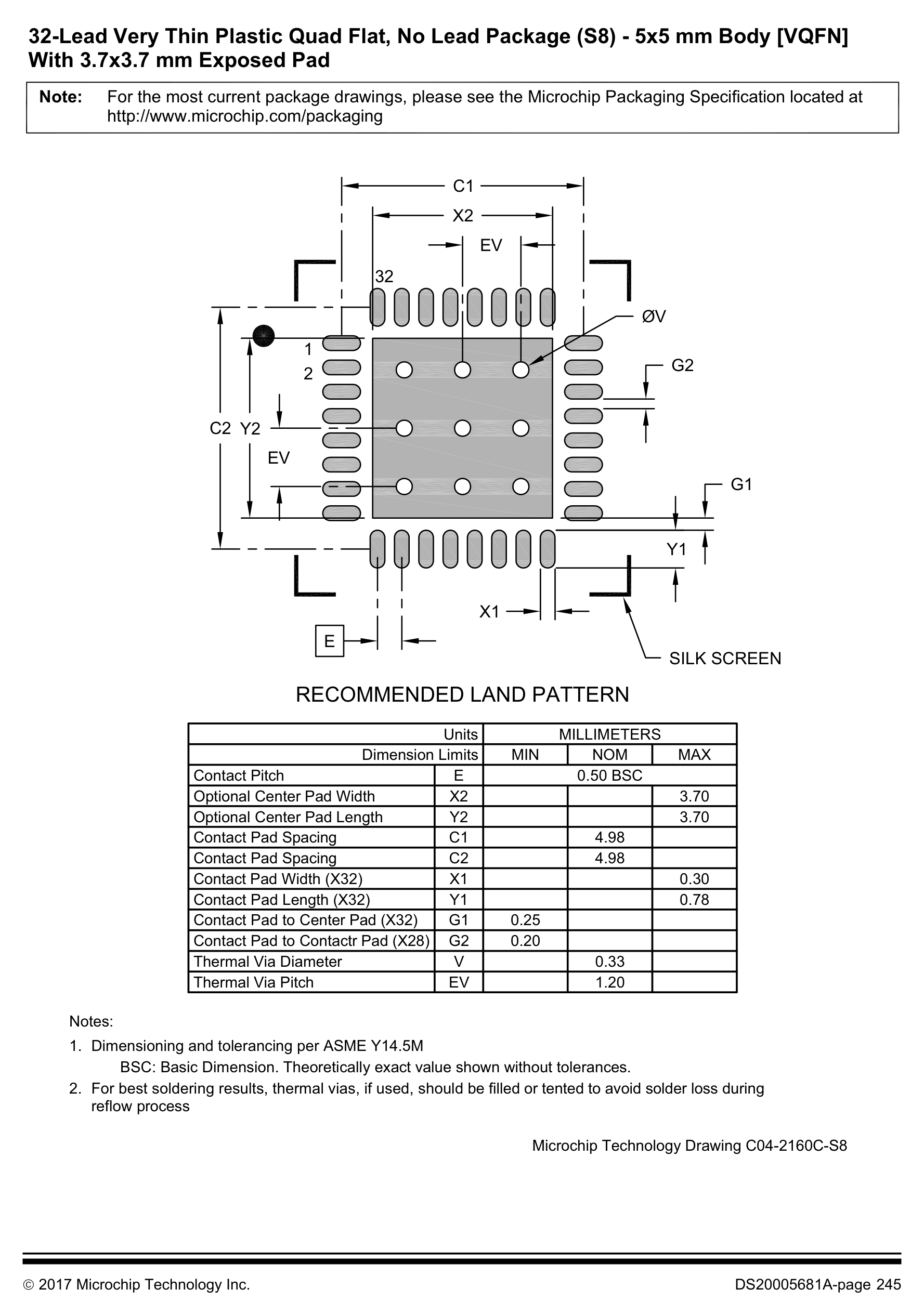
5. Recommended Land PatternLAND PATTERN
MCP19215T-E/S8 (QFN-32-EP(5x5)) - 5. Recommended Land Pattern
IPC-7351B Footprint (33 Pads)Expand ›
6. Application SchematicSCHEMATIC
MCP19215T-E/S8 (QFN-32-EP(5x5)) - 6. Application Schematic
Typical Application SchematicExpand ›
Original Datasheet Pinouts & Technical Drawings (21 figures · Page 1/2)
Showing 1–12 of 21 uncropped original figures for MCP19215
P1 · p01_fig01377×200px
MCP19215T-E/S8 (QFN-32-EP(5x5)) — Digitally Enhanced Power Analog, Dual Channel, Low-Side PWM
Digitally Enhanced Power Analog, Dual Channel, Low-Side PWM
P162 · p162_fig01872×966px
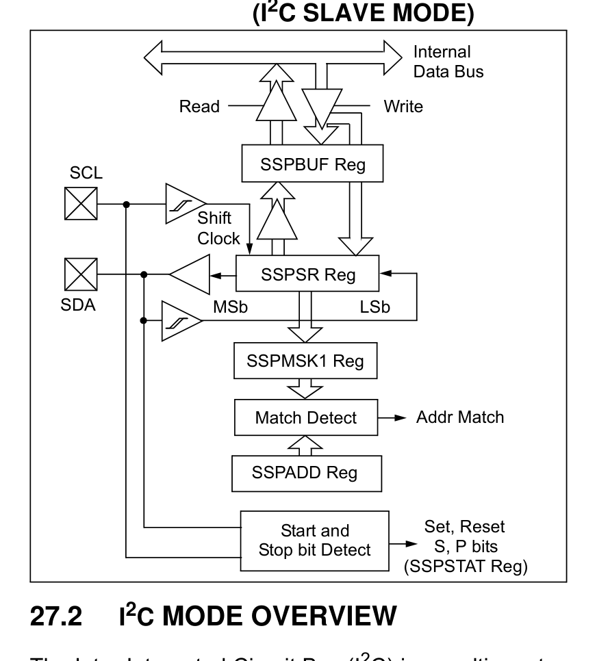
MCP19215T-E/S8 (QFN-32-EP(5x5)) — FIGURE 27-2: MSSP BLOCK DIAGRAM (I2C SLAVE MODE)
FIGURE 27-2: MSSP BLOCK DIAGRAM (I2C SLAVE MODE)
P162 · p162_fig02867×529px
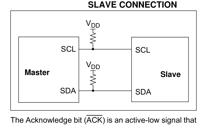
MCP19215T-E/S8 (QFN-32-EP(5x5)) — FIGURE 27-3: I2C MASTER/ SLAVE CONNECTION
FIGURE 27-3: I2C MASTER/ SLAVE CONNECTION
P215 · p215_fig01867×671px
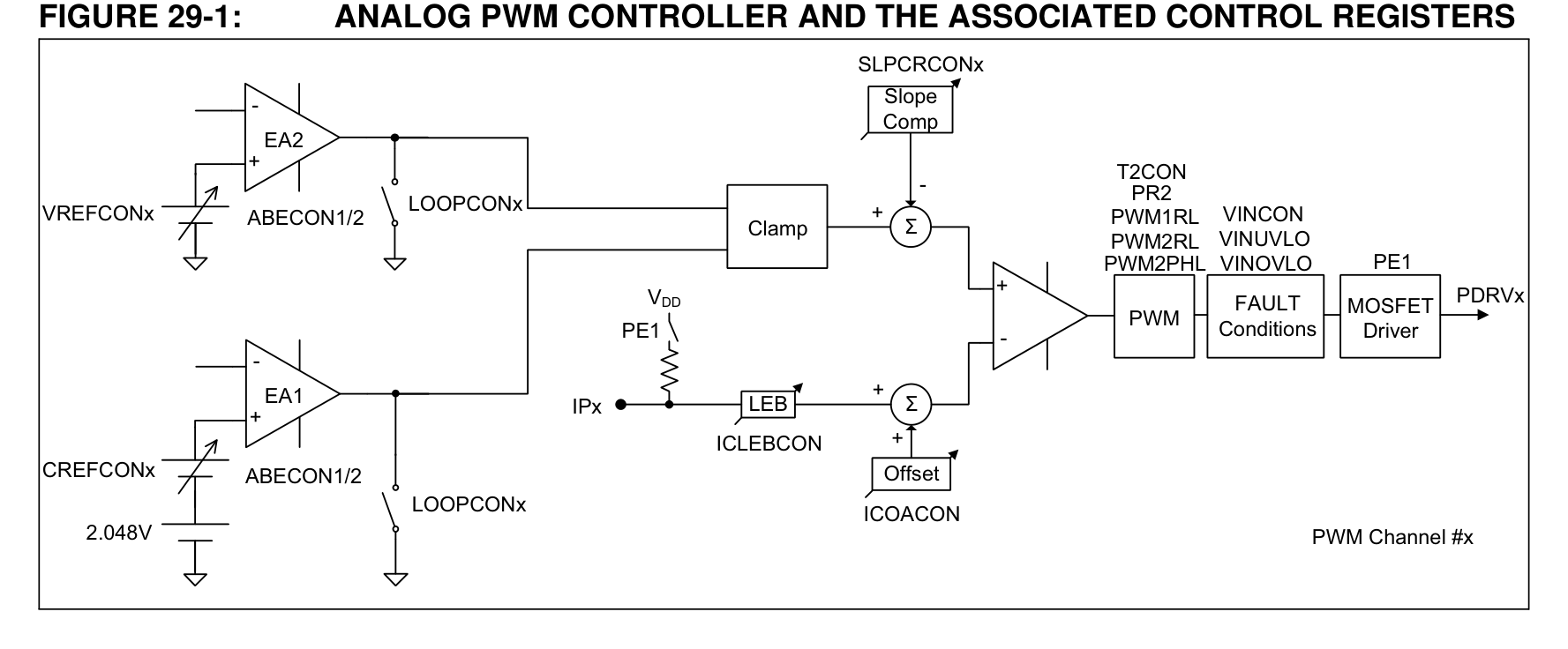
MCP19215T-E/S8 (QFN-32-EP(5x5)) — FIGURE 29-1: ANALOG PWM CONTROLLER AND THE ASSOCIATED CONTROL REGISTERS
FIGURE 29-1: ANALOG PWM CONTROLLER AND THE ASSOCIATED CONTROL REGISTERS
P215 · p215_fig021777×736px
MCP19215T-E/S8 (QFN-32-EP(5x5)) — FIGURE 29-1: ANALOG PWM CONTROLLER AND THE ASSOCIATED CONTROL REGISTERS
FIGURE 29-1: ANALOG PWM CONTROLLER AND THE ASSOCIATED CONTROL REGISTERS
P229 · p229_fig011644×893px
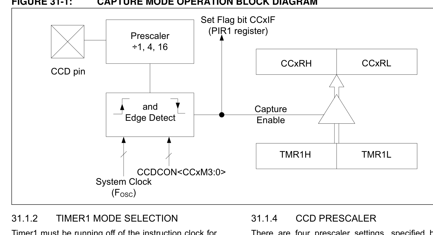
MCP19215T-E/S8 (QFN-32-EP(5x5)) — FIGURE 31-1: CAPTURE MODE OPERATION BLOCK DIAGRAM
FIGURE 31-1: CAPTURE MODE OPERATION BLOCK DIAGRAM
P230 · p230_fig011705×958px
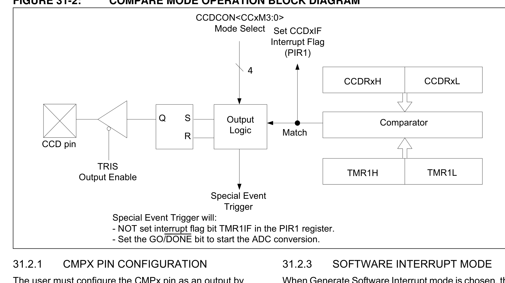
MCP19215T-E/S8 (QFN-32-EP(5x5)) — FIGURE 31-2: COMPARE MODE OPERATION BLOCK DIAGRAM
FIGURE 31-2: COMPARE MODE OPERATION BLOCK DIAGRAM
P230 · p230_fig021621×391px
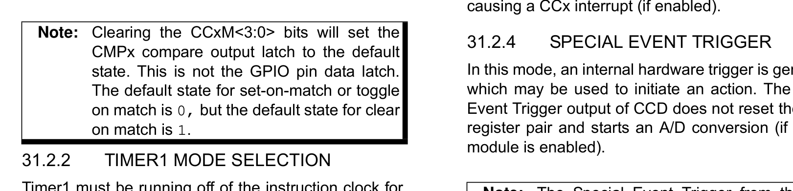
MCP19215T-E/S8 (QFN-32-EP(5x5)) — Note: The Special Event Trigger from the CCD module will not set the interrupt flag bit TMR1IF (bit 0 in the PIR1 register).
Note: The Special Event Trigger from the CCD module will not set the interrupt flag bit TMR1IF (bit 0 in the PIR1 register).
P234 · p234_fig011447×960px
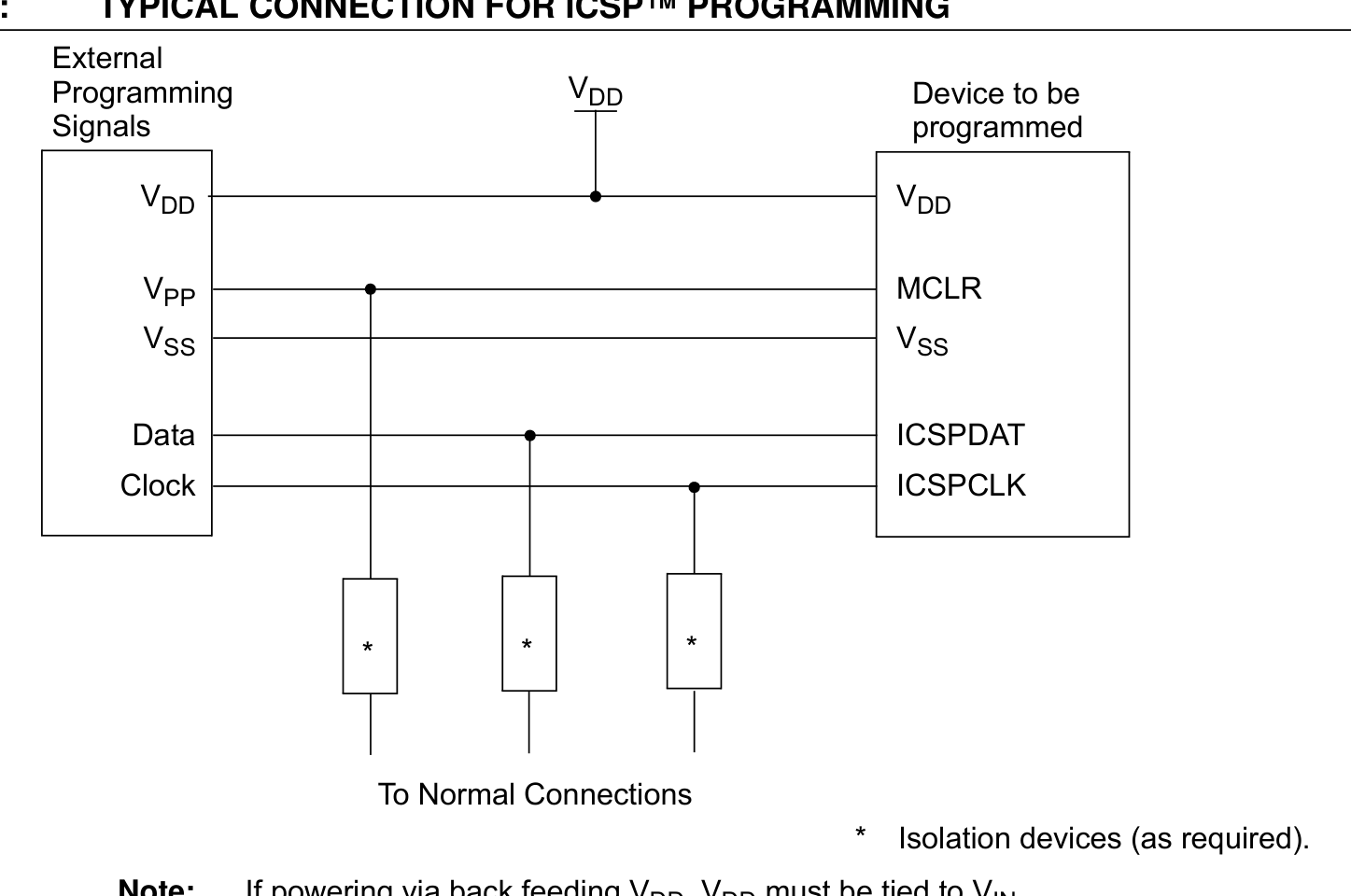
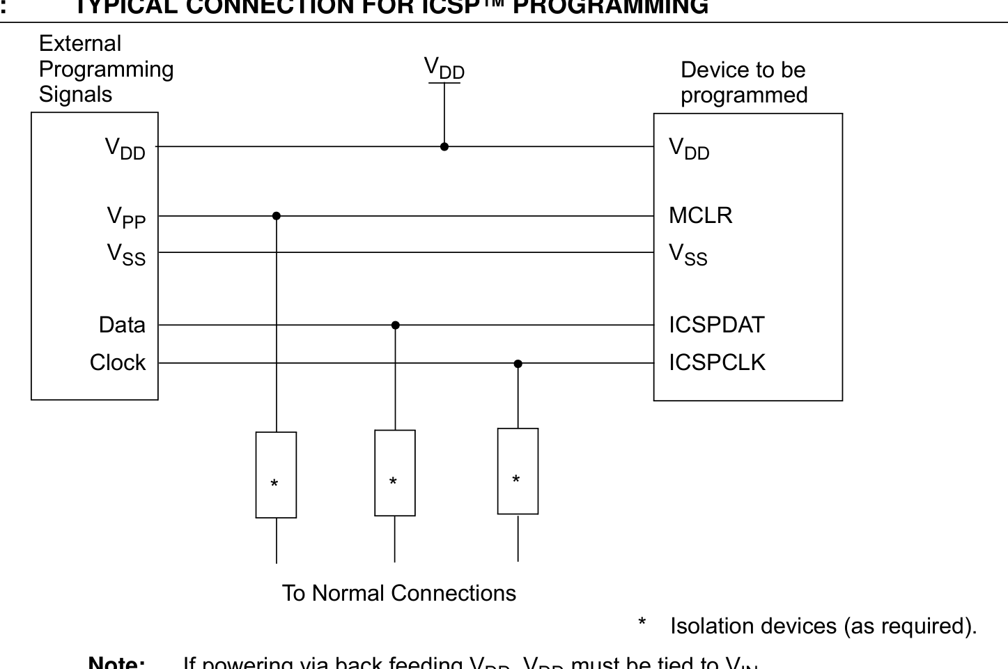
MCP19215T-E/S8 (QFN-32-EP(5x5)) — FIGURE 32-3: TYPICAL CONNECTION FOR ICSP™ PROGRAMMING
FIGURE 32-3: TYPICAL CONNECTION FOR ICSP™ PROGRAMMING
P234 · p234_fig01P234
MCP19215T-E/S8 (QFN-32-EP(5x5)) — Datasheet Page 234 (p234_fig01)
Datasheet Page 234 (p234_fig01)
P239 · p239_fig031652×1263px
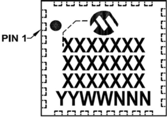
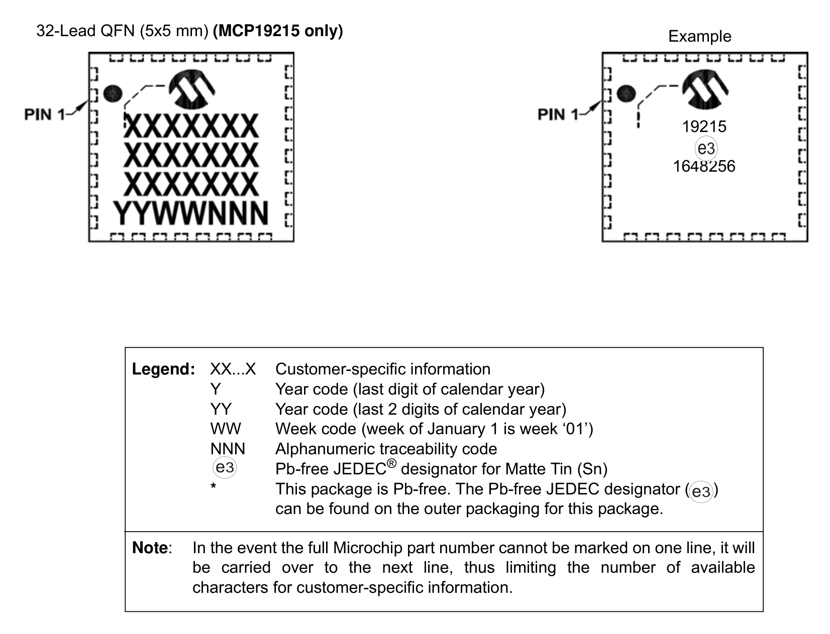
MCP19215T-E/S8 (QFN-32-EP(5x5)) — Note: In the event the full Microchip part number cannot be marked on one line, it will be carried over to the next line, thus limiting the number of available characters for customer-specific information. | 3 e | 3 e | Example 32-Lead QFN
Note: In the event the full Microchip part number cannot be marked on one line, it will be carried over to the next line, thus limiting the number of available characters for customer-specific information. | 3 e | 3 e | Example 32-Lead QFN
P239 · p239_fig04544×382px
MCP19215T-E/S8 (QFN-32-EP(5x5)) — Example 32-Lead QFN (5x5 mm) (MCP19215 only)
Example 32-Lead QFN (5x5 mm) (MCP19215 only)
Page 1 / 2 (21 extracted figures)

Technical Specifications & Part Details (MCP19215T-E/S8)

Summary of electrical parameters, mechanical dimensions, voltage range and peripheral interfaces from Datasheet (EN)
Standard Electronic & Interconnect Component
Detailed Overview:MCP19215T-E/S8 (QFN-32-EP(5x5)) is a 32-pin standard electronic & interconnect component featuring a 5.00 × 5.00 × 0.90 mm mechanical envelope (lead pitch e = 0.50 mm). Rated for 4.5V-42V supply operation across 40°C to +125°C with integrated I2C, ADC, DAC, PWM interfaces.
Operating Supply VoltageV_CC / V_DD
4.5V-42V
Place 100nF + 10µF X7R decoupling capacitors < 2mm from supply pins
Ambient Operating TemperatureT_A
40°C to +125°C
Industrial temperature grade; T_J(max) = +125°C
Clock / RF Operating Frequencyf_CLK / f_RF
31.25 kHz
Extracted from authoritative PDF specification tables
Current & Power RatingI_OUT / I_CC
10 mA
Observe per-pin absolute maximum current limits
Package Envelope (D × E × A)D × E × A
5.00 × 5.00 × 0.90 mm (A1=0.03 mm)
Package family: QFN (QFN-32-EP(5x5))
Pin Count & Lead PitchN / e
32 Pins | Pitch e = 0.50 mm (19.7 mil)
Normalized to Center-to-Center Span C per IPC-7351B
Integrated Peripheral InterfacesBuses
I2C, ADC, DAC, PWM
Cross-linked with 4D Pinout & Schematic Symbol
Reflow & Moisture SensitivityIPC / MSL
IPC-7351B Level B | J-STD-020 (Peak 260°C) | MSL-3
60% windowed solder paste stencil on thermal EPAD
Engineering Safety Alert: Verify Pin-1 chamfer orientation on Top Silkscreen prior to SMT pick-and-place assembly.
Engineering Safety Alert: Connect exposed thermal pad (if present) to internal ground plane via 0.3mm stitched thermal vias.

5-Point Standards Verification

Automated compliance checks prior to export
5/5 PASS
IEEE-315 Symbol33 auto-grouped pins
OK
IPC-7351B Land Pattern33 pads · Pitch 0.50mm
OK
IPC-7525 60% Solder PasteEPAD 3.80×3.80mm windowed grid
OK
DFM Rules JLCPCB / PCBWayMin pad clearance: 0.25mm
OK
3D STEP AP214 & GLBAligned coordinate origin (0,0,0)
OK

Hardware Verification & Community Engineering Reviews

Summary of electrical parameters, mechanical dimensions, voltage range and peripheral interfaces from Datasheet
5.00 PCB Verified

Mechanical Dimensions & Land Pattern (QFN-32-EP(5x5))

Extracted from Datasheet & IPC-7351B Normalized
mm
Package Body (D × E)Nominal
5.00 × 5.00 mm
Height (A) & Pitch (e)IPC-7351B
A=0.90mm · e=0.50mm
Pad Size (W × L)Level B
0.30 × 0.80 mm
Pins / Total PadsTopology
33P / 33Pad (QUAD_ROW)

Recommended Companion BOM & Drop-In Equivalents

Passive external components per reference schematic and 1:1 pin-compatible alternatives
DFM READY
Designator / Replacement MPNValue / PackageFunction & PCB Layout Rule
N/A
BOM
Per application circuit
QFN-32-EP(5x5)
Size power & signal trace widths for rated load current following IPC-2221 clearance rules.

Technical Frequently Asked Questions (FAQ) — MCP19215T-E/S8 (QFN-32-EP(5x5))

Quick answers covering Pinout, IPC-7351B Land Pattern dimensions, and CAD export formats
IPC-7351B / IEEE-315

What is the Pinout and operating voltage specification of MCP19215T-E/S8 (QFN-32-EP(5x5))?

Manufactured by MICROCHIP, the MCP19215T-E/S8 is housed in a QFN-32-EP(5x5) package with 33 pins and a 0.50 mm lead pitch, supporting a VCC supply range of 4.5V-42V. Key pins include: 1 (GPA0/AN0/TS_OUT1: Multiplexed I/O & Peripheral Pin GPA0/AN0/TS_OUT1 (General)), 2 (GPA1/AN1: Multiplexed I/O & Peripheral Pin GPA1/AN1 (General)), 3 (GPA2/AN2/T0CKI/INT: Multiplexed I/O & Peripheral Pin GPA2/AN2/T0CKI/INT (General)), 4 (GPB4/AN5/ICSPDAT: Multiplexed I/O & Peripheral Pin GPB4/AN5/ICSPDAT (General)), 5 (GPA3/AN3/TS_OUT2: Multiplexed I/O & Peripheral Pin GPA3/AN3/TS_OUT2 (General)), 6 (GPA7/SCL: Multiplexed I/O & Peripheral Pin GPA7/SCL (I2C)).

What are the IPC-7351B PCB Footprint dimensions for MCP19215T-E/S8?

Normalized from the official datasheet mechanical drawing per IPC-7351B (Density Level B Nominal), MCP19215T-E/S8 (QFN-32-EP(5x5)) has a nominal body envelope of 5.00 × 5.00 mm, pitch e = 0.50 mm, and 33 copper pads plus a central exposed thermal pad (EPAD) of 3.80 × 3.80 mm with a 60% IPC-7525 windowed solder paste grid.

Where can I download KiCad (.kicad_mod, .kicad_sym), Fusion 360 (.lbr), and 3D STEP models for MCP19215T-E/S8?

You can download the verified open-hardware (CERN-OHL-P-2.0) CAD library bundle for MCP19215T-E/S8 (MICROCHIP, QFN-32-EP(5x5)) directly on this page, including KiCad 8 Footprints (.kicad_mod), Schematic Symbols (.kicad_sym), Autodesk Fusion 360 / Eagle (.lbr), and 3D STEP AP214 / WebGL GLB models.

Static Reference Appendix: Pinout Table (33 pins) & MCP19215 Family VariantsExpand static table
Pin #Signal NameElectrical TypeFunctional Description & Design Notes
1GPA0/AN0/TS_OUT1Digital_IOSignal terminal GPA0/AN0/TS_OUT1 (I/O, 4.5V-42V domain). Multiplexed alternate functions: GPA0/AN0/TS_OUT1. Supported peripheral buses: General.
2GPA1/AN1Digital_IOSignal terminal GPA1/AN1 (I/O, 4.5V-42V domain). Multiplexed alternate functions: GPA1/AN1. Supported peripheral buses: General.
3GPA2/AN2/T0CKI/INTDigital_IOSignal terminal GPA2/AN2/T0CKI/INT (I/O, 4.5V-42V domain). Multiplexed alternate functions: GPA2/AN2/T0CKI/INT. Supported peripheral buses: General.
4GPB4/AN5/ICSPDATDigital_IOSignal terminal GPB4/AN5/ICSPDAT (I/O, 4.5V-42V domain). Multiplexed alternate functions: GPB4/AN5/ICSPDAT. Supported peripheral buses: General.
5GPA3/AN3/TS_OUT2Digital_IOSignal terminal GPA3/AN3/TS_OUT2 (I/O, 4.5V-42V domain). Multiplexed alternate functions: GPA3/AN3/TS_OUT2. Supported peripheral buses: General.
6GPA7/SCLDigital_IOSignal terminal GPA7/SCL (I/O, 4.5V-42V domain). Multiplexed alternate functions: GPA7/SCL. Supported peripheral buses: I2C.
7GPB0/SDADigital_IOSignal terminal GPB0/SDA (I/O, 4.5V-42V domain). Multiplexed alternate functions: GPB0/SDA. Supported peripheral buses: I2C.
8GPA5/MCLRDigital_IOSignal terminal GPA5/MCLR (I/O, 4.5V-42V domain). Multiplexed alternate functions: GPA5/MCLR. Supported peripheral buses: General.
9GPB7/CCD2Digital_IOSignal terminal GPB7/CCD2 (I/O, 4.5V-42V domain). Multiplexed alternate functions: GPB7/CCD2. Supported peripheral buses: General.
10GPA6/CCD1Digital_IOSignal terminal GPA6/CCD1 (I/O, 4.5V-42V domain). Multiplexed alternate functions: GPA6/CCD1. Supported peripheral buses: General.
11AGND/DGNDGND0V electrical ground return terminal (AGND/DGND) for internal core logic, I/O drivers, and analog sub-blocks.
12ISN2Digital_IOSignal terminal ISN2 (I/O, 4.5V-42V domain). Multiplexed alternate functions: ISN2. Supported peripheral buses: General.
13ISP2Digital_IOSignal terminal ISP2 (I/O, 4.5V-42V domain). Multiplexed alternate functions: ISP2. Supported peripheral buses: General.
14CCOMP2Digital_IOSignal terminal CCOMP2 (I/O, 4.5V-42V domain). Multiplexed alternate functions: CCOMP2. Supported peripheral buses: General.
15VCOMP2Digital_IOSignal terminal VCOMP2 (I/O, 4.5V-42V domain). Multiplexed alternate functions: VCOMP2. Supported peripheral buses: General.
16VFB2Digital_IOSignal terminal VFB2 (I/O, 4.5V-42V domain). Multiplexed alternate functions: VFB2. Supported peripheral buses: General.
17IP2Digital_IOSignal terminal IP2 (I/O, 4.5V-42V domain). Multiplexed alternate functions: IP2. Supported peripheral buses: General.
18PDRV2Digital_IOSignal terminal PDRV2 (I/O, 4.5V-42V domain). Multiplexed alternate functions: PDRV2. Supported peripheral buses: General.
19PGNDGND0V electrical ground return terminal (PGND) for internal core logic, I/O drivers, and analog sub-blocks.
20PDRV1Digital_IOSignal terminal PDRV1 (I/O, 4.5V-42V domain). Multiplexed alternate functions: PDRV1. Supported peripheral buses: General.
21VDRDigital_IOSignal terminal VDR (I/O, 4.5V-42V domain). Multiplexed alternate functions: VDR. Supported peripheral buses: General.
22VDDPower_InPrimary positive power supply input (VDD) operating in the 4.5V-42V domain (Max rating: 42.0V).
23VINPower_InPrimary positive power supply input (VIN) operating in the 4.5V-42V domain (Max rating: 42.0V).
24IP1Digital_IOSignal terminal IP1 (I/O, 4.5V-42V domain). Multiplexed alternate functions: IP1. Supported peripheral buses: General.
25VFB1Digital_IOSignal terminal VFB1 (I/O, 4.5V-42V domain). Multiplexed alternate functions: VFB1. Supported peripheral buses: General.
26VCOMP1Digital_IOSignal terminal VCOMP1 (I/O, 4.5V-42V domain). Multiplexed alternate functions: VCOMP1. Supported peripheral buses: General.
27CCOMP1Digital_IOSignal terminal CCOMP1 (I/O, 4.5V-42V domain). Multiplexed alternate functions: CCOMP1. Supported peripheral buses: General.
28ISP1Digital_IOSignal terminal ISP1 (I/O, 4.5V-42V domain). Multiplexed alternate functions: ISP1. Supported peripheral buses: General.
29ISN1Digital_IOSignal terminal ISN1 (I/O, 4.5V-42V domain). Multiplexed alternate functions: ISN1. Supported peripheral buses: General.
30GPB6/AN7/TX/CKDigital_IOSignal terminal GPB6/AN7/TX/CK (I/O, 4.5V-42V domain). Multiplexed alternate functions: GPB6/AN7/TX/CK. Supported peripheral buses: General.
31GPB1/AN4/RX/DTDigital_IOSignal terminal GPB1/AN4/RX/DT (I/O, 4.5V-42V domain). Multiplexed alternate functions: GPB1/AN4/RX/DT. Supported peripheral buses: General.
32GPB5/AN6/ICSPCLKDigital_IOSignal terminal GPB5/AN6/ICSPCLK (I/O, 4.5V-42V domain). Multiplexed alternate functions: GPB5/AN6/ICSPCLK. Supported peripheral buses: General.
33EPADGNDBottom exposed die attach pad (EPAD) providing primary thermal conduction path to the PCB and low-inductance 0V ground return.