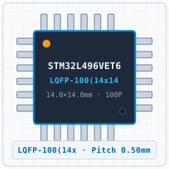
STM32L496VET6 (LQFP-100(14x14)) — Symbol, Footprint IPC-7351B & 3D STEP Model

STM32L496VET6

STID: C1337422LQFP-100(14x14) · 100 Pins · Pitch 0.50mmIPC TOLERANCE VARIATION5.0 (0)
SYNCHRONIZED 4D CROSS-PROBE MODETouch or hover any pin to highlight concurrently across Symbol, Footprint and 3D
1. SYMBOL
U1 · STM32L496VET6 (LQFP-100(14x14))1PE22PE33PE44PE55PE66VBAT7PC138PC14 - OSC329IO410VSS11VDD12PH0OSC IN -_13PH1 - OSC_OU14NRST15PC016PC117PC218PC319VSSA/VREF -20VREF -21VREF+22VDDA23PA024PA125PA226PA327VSS28VDD29PA430PA531PA632PA733PC434PC535PB036PB137PB238PE739PE840PE941PE1042PE1143PE1244PE1345PE1446PE1547PB1048PB1149VSS50VDD100VDD99VSS98PE197PE096PB995PB894PH3BOOT0 -93PB792PB691PB590PB4(NJTRST)89PB3 (JTDO/TR88PD787PD686PD585PD484PD383PD282PD181PD080PC1279PC1178PC1077PA15(JTDI)76PA14(JTCK/ S75VDD74VSS73VDDUSB72PA13(JTMS/ S71PA1270PA1169PA1068PA967PA866PC965PC864PC763PC662PD1561PD1460PD1359PD1258PD1157PD1056PD955PD854PB1553PB1452PB1351PB12Grid Pitch = 2.54mm (IEEE-315)-17.8-12.7-7.6-2.52.57.612.717.868.663.558.453.348.343.238.133.027.922.917.812.77.62.5-2.5-7.6-12.7-17.8-22.9-27.9-33.0-38.1-43.2-48.3-53.3-58.4-63.5-68.6mm
2. 2D FOOTPRINT
123456789101112131415161718192021222324252627282930313233343536373839404142434445464748495051525354555657585960616263646566676869707172737475767778798081828384858687888990919293949596979899100E=14.00mm · Pitch e=0.50mmD=14.00mm-13-11-9-7-5-3-1135791113131197531-1-3-5-7-9-11-13mm
3. 3D CAD MODEL
Package Body: 14.00mm × 14.00mm · Pitch: 0.50mm · Ruler Step: 1.00mmSynced <100ms

Synchronized Pinout (Symbol / 2D / 3D) (100/100)

Touch or hover any pin to highlight concurrently across Symbol, Footprint and 3D
PinSymbolTypeFunction (EN)
1PE2I/OMultiplexed I/O & Peripheral Pin PE2 (General)
2PE3I/OMultiplexed I/O & Peripheral Pin PE3 (General)
3PE4I/OMultiplexed I/O & Peripheral Pin PE4 (General)
4PE5I/OMultiplexed I/O & Peripheral Pin PE5 (General)
5PE6I/OMultiplexed I/O & Peripheral Pin PE6 (I2C, RTC/CLK)
6VBATPowerPower Supply Input (VBAT — 3.3V VDD (Max 4.0V))
7PC13I/OMultiplexed I/O & Peripheral Pin PC13 (RTC/CLK)
8PC14 - OSC32_IN (PC14)I/OMultiplexed I/O & Peripheral Pin PC14 - OSC32_IN (PC14) (RTC/CLK)
9IO4I/OGPIO4 / RTC_GPIO4 / TOUCH4 / ADC1_CH3
10VSSGNDGround Reference Pin (VSS)
11VDDPowerPower Supply Input (VDD — 3.3V VDD (Max 4.0V))
12PH0OSC IN -_ (PH0)I/OMultiplexed I/O & Peripheral Pin PH0OSC IN -_ (PH0) (RTC/CLK)
13PH1 - OSC_OUT (PH1)I/OMultiplexed I/O & Peripheral Pin PH1 - OSC_OUT (PH1) (RTC/CLK)
14NRSTISystem Enable & Hardware Reset (NRST)
15PC0I/OMultiplexed I/O & Peripheral Pin PC0 (I2C, ADC)
16PC1I/OMultiplexed I/O & Peripheral Pin PC1 (I2C, ADC)
17PC2I/OMultiplexed I/O & Peripheral Pin PC2 (SPI, ADC)
18PC3I/OMultiplexed I/O & Peripheral Pin PC3 (SPI, ADC)
19VSSA/VREF -GNDGround Reference Pin (VSSA/VREF -)
20VREF -AnalogMultiplexed I/O & Peripheral Pin VREF - (General)
21VREF+AnalogMultiplexed I/O & Peripheral Pin VREF+ (General)
22VDDAPowerPower Supply Input (VDDA — 3.3V VDD (Max 4.0V))
23PA0I/OMultiplexed I/O & Peripheral Pin PA0 (UART, ADC, PWM, RTC/CLK)
24PA1I/OMultiplexed I/O & Peripheral Pin PA1 (UART, I2C, ADC, PWM)
25PA2I/OMultiplexed I/O & Peripheral Pin PA2 (UART, ADC, PWM)
26PA3I/OMultiplexed I/O & Peripheral Pin PA3 (UART, ADC, PWM)
27VSSGNDGround Reference Pin (VSS)
28VDDPowerPower Supply Input (VDD — 3.3V VDD (Max 4.0V))
29PA4I/OMultiplexed I/O & Peripheral Pin PA4 (UART, SPI, ADC, DAC)
30PA5I/OMultiplexed I/O & Peripheral Pin PA5 (ADC, DAC, PWM)
31PA6I/OMultiplexed I/O & Peripheral Pin PA6 (UART, SPI, ADC)
32PA7I/OMultiplexed I/O & Peripheral Pin PA7 (SPI, ADC, PWM)
33PC4I/OMultiplexed I/O & Peripheral Pin PC4 (UART, ADC)
34PC5I/OMultiplexed I/O & Peripheral Pin PC5 (UART, ADC)
35PB0I/OMultiplexed I/O & Peripheral Pin PB0 (UART, ADC, PWM)
36PB1I/OMultiplexed I/O & Peripheral Pin PB1 (UART, ADC, PWM)
37PB2I/OMultiplexed I/O & Peripheral Pin PB2 (I2C, RTC/CLK)
38PE7I/OMultiplexed I/O & Peripheral Pin PE7 (General)
39PE8I/OMultiplexed I/O & Peripheral Pin PE8 (PWM)
40PE9I/OMultiplexed I/O & Peripheral Pin PE9 (PWM)
41PE10I/OMultiplexed I/O & Peripheral Pin PE10 (PWM)
42PE11I/OMultiplexed I/O & Peripheral Pin PE11 (PWM)
43PE12I/OMultiplexed I/O & Peripheral Pin PE12 (PWM)
44PE13I/OMultiplexed I/O & Peripheral Pin PE13 (PWM)
45PE14I/OMultiplexed I/O & Peripheral Pin PE14 (SPI, PWM)
46PE15I/OMultiplexed I/O & Peripheral Pin PE15 (SPI)
47PB10I/OMultiplexed I/O & Peripheral Pin PB10 (UART, SPI, I2C, PWM)
48PB11I/OMultiplexed I/O & Peripheral Pin PB11 (UART, I2C, PWM)
49VSSGNDExposed Thermal & Ground Pad (VSS)
50VDDPowerPower Supply Input (VDD — 3.3V VDD (Max 4.0V))
51PB12I/OMultiplexed I/O & Peripheral Pin PB12 (UART, I2C, CAN)
52PB13I/OMultiplexed I/O & Peripheral Pin PB13 (UART, SPI, PWM)
53PB14I/OMultiplexed I/O & Peripheral Pin PB14 (UART, SPI, PWM)
54PB15I/OMultiplexed I/O & Peripheral Pin PB15 (SPI, I2C, PWM, RTC/CLK)
55PD8I/OMultiplexed I/O & Peripheral Pin PD8 (UART)
56PD9I/OMultiplexed I/O & Peripheral Pin PD9 (UART)
57PD10I/OMultiplexed I/O & Peripheral Pin PD10 (UART, SPI)
58PD11I/OMultiplexed I/O & Peripheral Pin PD11 (UART, I2C)
59PD12I/OMultiplexed I/O & Peripheral Pin PD12 (UART, PWM)
60PD13I/OMultiplexed I/O & Peripheral Pin PD13 (PWM)
61PD14I/OMultiplexed I/O & Peripheral Pin PD14 (PWM)
62PD15I/OMultiplexed I/O & Peripheral Pin PD15 (PWM)
63PC6I/OMultiplexed I/O & Peripheral Pin PC6 (PWM)
64PC7I/OMultiplexed I/O & Peripheral Pin PC7 (PWM)
65PC8I/OMultiplexed I/O & Peripheral Pin PC8 (PWM)
66PC9I/OMultiplexed I/O & Peripheral Pin PC9 (I2C, PWM)
67PA8I/OMultiplexed I/O & Peripheral Pin PA8 (UART, SPI, RTC/CLK)
68PA9I/OMultiplexed I/O & Peripheral Pin PA9 (PWM)
69PA10I/OMultiplexed I/O & Peripheral Pin PA10 (UART, I2C, PWM)
70PA11I/OMultiplexed I/O & Peripheral Pin PA11 (UART, SPI, PWM, CAN)
71PA12I/OMultiplexed I/O & Peripheral Pin PA12 (UART, CAN)
72PA13(JTMS/ SWDIO)I/OMultiplexed I/O & Peripheral Pin PA13(JTMS/ SWDIO) (SWD/JTAG)
73VDDUSBPowerPower Supply Input (VDDUSB — 3.3V VDD (Max 4.0V))
74VSSGNDGround Reference Pin (VSS)
75VDDPowerPower Supply Input (VDD — 3.3V VDD (Max 4.0V))
76PA14(JTCK/ SWCLK)I/OMultiplexed I/O & Peripheral Pin PA14(JTCK/ SWCLK) (I2C, SWD/JTAG)
77PA15(JTDI)I/OMultiplexed I/O & Peripheral Pin PA15(JTDI) (UART, SPI, SWD/JTAG)
78PC10I/OMultiplexed I/O & Peripheral Pin PC10 (UART, SPI)
79PC11I/OMultiplexed I/O & Peripheral Pin PC11 (UART, SPI)
80PC12I/OMultiplexed I/O & Peripheral Pin PC12 (UART, SPI)
81PD0I/OMultiplexed I/O & Peripheral Pin PD0 (SPI, CAN)
82PD1I/OMultiplexed I/O & Peripheral Pin PD1 (SPI, CAN)
83PD2I/OMultiplexed I/O & Peripheral Pin PD2 (UART)
84PD3I/OMultiplexed I/O & Peripheral Pin PD3 (UART, SPI)
85PD4I/OMultiplexed I/O & Peripheral Pin PD4 (UART, SPI)
86PD5I/OMultiplexed I/O & Peripheral Pin PD5 (UART)
87PD6I/OMultiplexed I/O & Peripheral Pin PD6 (UART, I2C)
88PD7I/OMultiplexed I/O & Peripheral Pin PD7 (UART)
89PB3 (JTDO/TRACE SWO)I/OMultiplexed I/O & Peripheral Pin PB3 (JTDO/TRACE SWO) (UART, SPI, PWM, SWD/JTAG)
90PB4(NJTRST)I/OMultiplexed I/O & Peripheral Pin PB4(NJTRST) (UART, SPI, I2C, SWD/JTAG)
91PB5I/OMultiplexed I/O & Peripheral Pin PB5 (UART, SPI, CAN)
92PB6I/OMultiplexed I/O & Peripheral Pin PB6 (UART, I2C, PWM)
93PB7I/OMultiplexed I/O & Peripheral Pin PB7 (UART, I2C)
94PH3BOOT0 -I/OMultiplexed I/O & Peripheral Pin PH3BOOT0 - (General)
95PB8I/OMultiplexed I/O & Peripheral Pin PB8 (UART, PWM, CAN)
96PB9I/OMultiplexed I/O & Peripheral Pin PB9 (UART, I2C, CAN)
97PE0I/OMultiplexed I/O & Peripheral Pin PE0 (General)
98PE1I/OMultiplexed I/O & Peripheral Pin PE1 (General)
99VSSGNDGround Reference Pin (VSS)
100VDDPowerPower Supply Input (VDD — 3.3V VDD (Max 4.0V))
PIN 1 PE2
I/O
Multiplexed I/O & Peripheral Pin PE2 (General)
Design note: Alt: TRACECK TIM3 ETR ,_ , TSC_G7IO1_ , LCD_SEG38FMCA23 ,_ , SAI1_MCLKA_ , EVENTOUT
IPC-7351B Solder Density & Span C/G/Z Tuner

Live Embedded Datasheet PDF & Technical Drawing Gallery (6 Standard Drawings + 15 Extracted Figures)

Read the original datasheet PDF directly or click any drawing to view fullscreen
Open PDF in New Window ↗Read Datasheet PDF (.pdf)
PDF VIEWEROfficial Datasheet Document: STM32L496VET6 (ST · LQFP-100(14x14))
Scroll, search text (Ctrl+F), or expand directly inside the embedded PDF reader below
1. Realistic 3D PackageREPRESENTATIVE
STM32L496VET6 (LQFP-100(14x14)) - 1. Realistic 3D Package
Detailed solid 3D bodyExpand ›
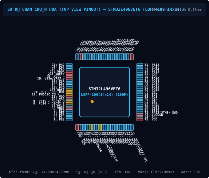
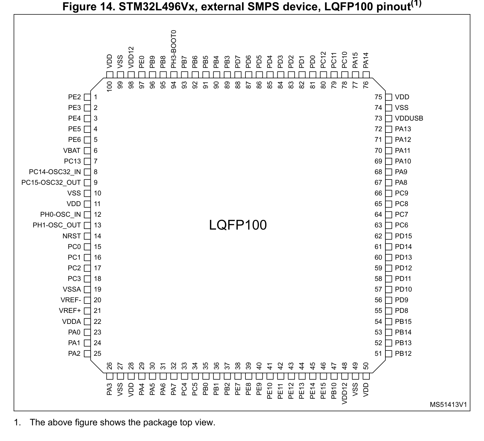
2. Standard Pinout (Top View)CLEANROOM PINOUT
STM32L496VET6 (LQFP-100(14x14)) - 2. Standard Pinout (Top View)
True package pinout (100 pins)Expand ›
3. Original Datasheet PinoutPDF PINOUT
STM32L496VET6 (LQFP-100(14x14)) - 3. Original Datasheet Pinout
Uncropped datasheet pin diagramExpand ›
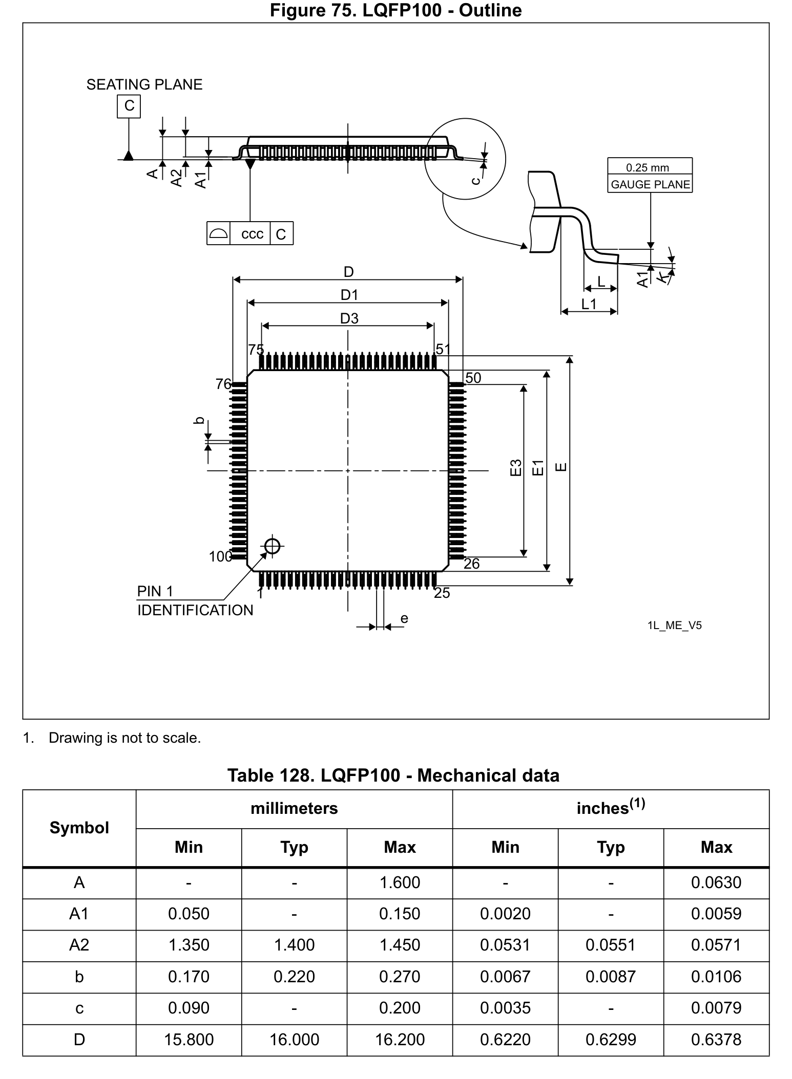
4. Package Dimensions (D×E×A)PACKAGE DIMENSIONS
STM32L496VET6 (LQFP-100(14x14)) - 4. Package Dimensions (D×E×A)
LQFP-100(14x14) · 14.00×14.00mm · Pitch 0.50mmExpand ›
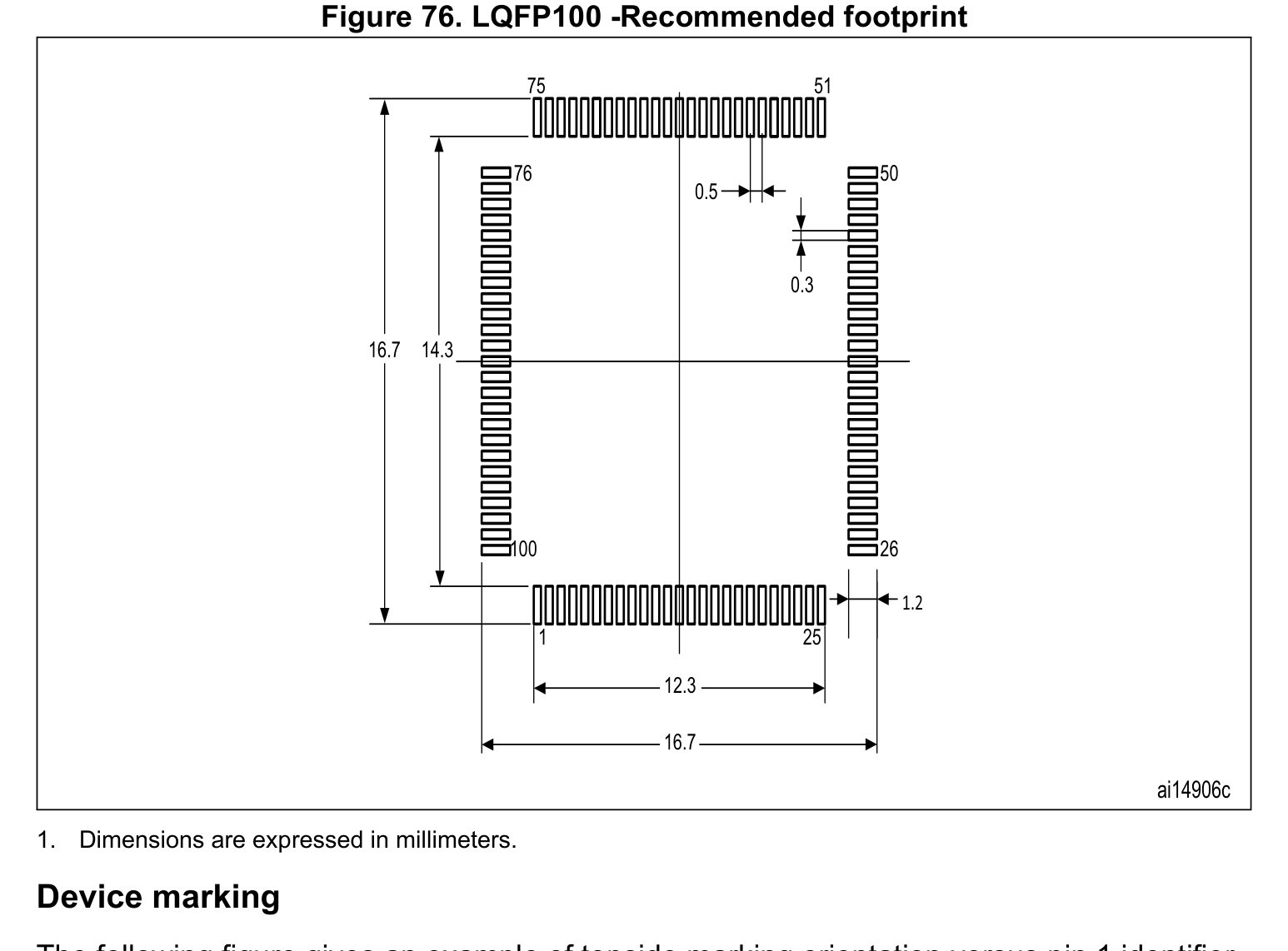
5. Recommended Land PatternLAND PATTERN
STM32L496VET6 (LQFP-100(14x14)) - 5. Recommended Land Pattern
IPC-7351B Footprint (100 Pads)Expand ›
6. Application SchematicSCHEMATIC
STM32L496VET6 (LQFP-100(14x14)) - 6. Application Schematic
Typical Application SchematicExpand ›
Original Datasheet Pinouts & Technical Drawings (15 figures · Page 1/2)
Showing 1–12 of 15 uncropped original figures for STM32L496
P66 · p66_fig01EXACT PACKAGE
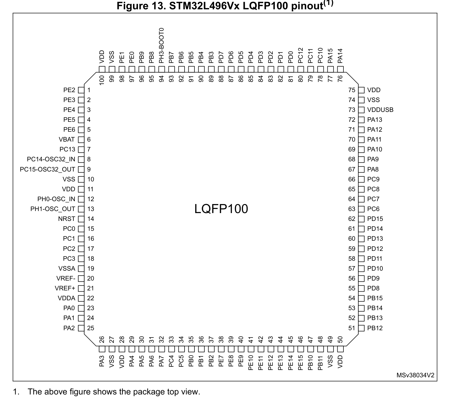
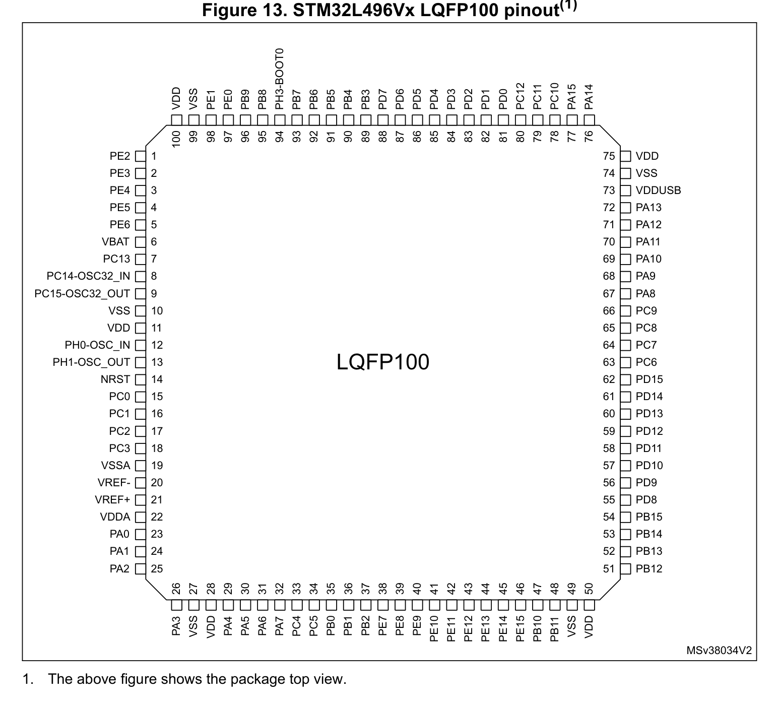
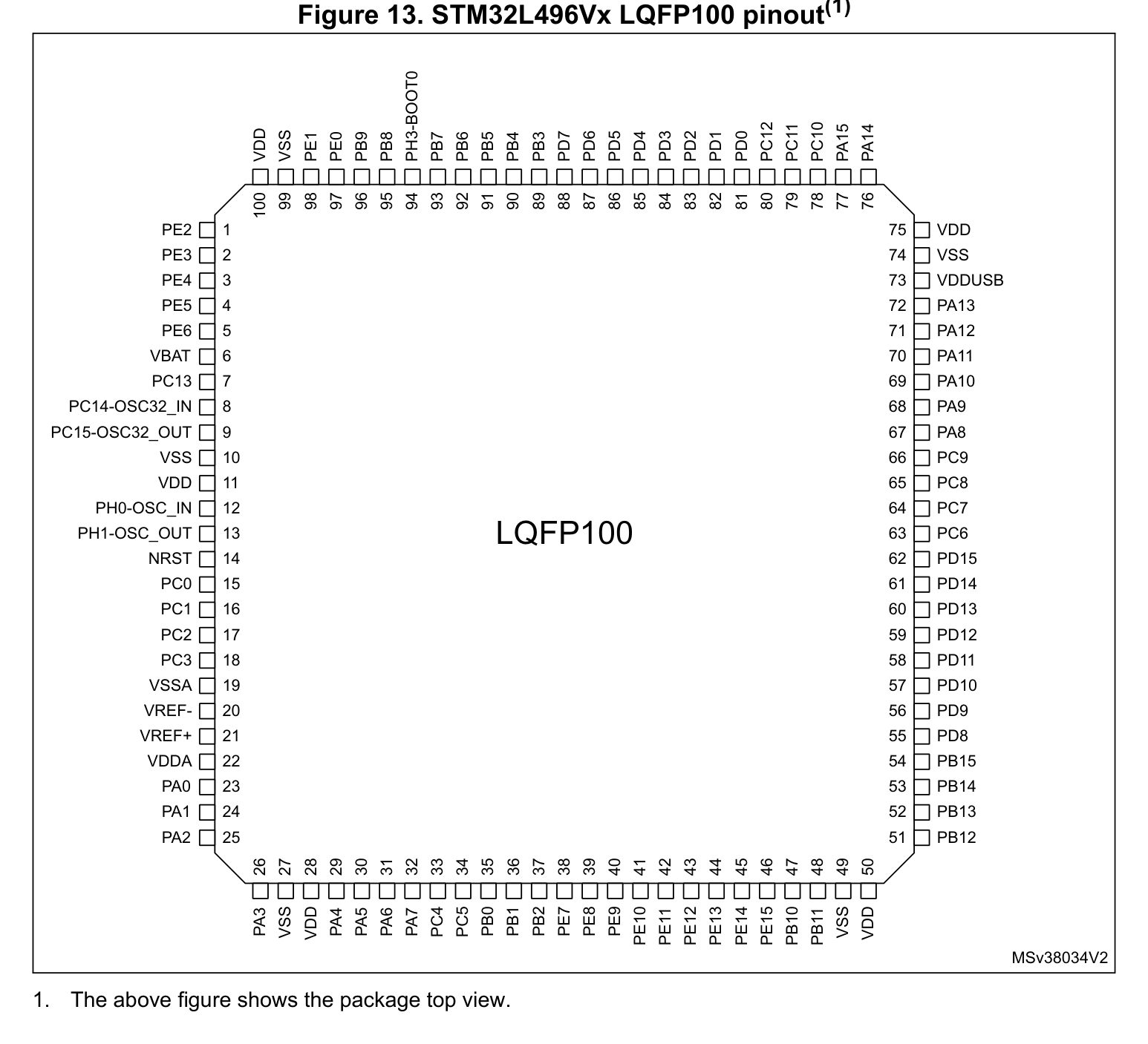
STM32L496VET6 (LQFP-100(14x14)) — Figure 13. STM32L496Vx LQFP100 pinout(1)
Figure 13. STM32L496Vx LQFP100 pinout(1)
P67 · p67_fig01EXACT PACKAGE
STM32L496VET6 (LQFP-100(14x14)) — Figure 14. STM32L496Vx, external SMPS device, LQFP100 pinout(1)
Figure 14. STM32L496Vx, external SMPS device, LQFP100 pinout(1)
P264 · p264_fig01EXACT PACKAGE
STM32L496VET6 (LQFP-100(14x14)) — Figure 75. LQFP100 - Outline
Figure 75. LQFP100 - Outline
P265 · p265_fig01EXACT PACKAGE
STM32L496VET6 (LQFP-100(14x14)) — Figure 76. LQFP100 -Recommended footprint
Figure 76. LQFP100 -Recommended footprint
P266 · p266_fig01EXACT PACKAGE
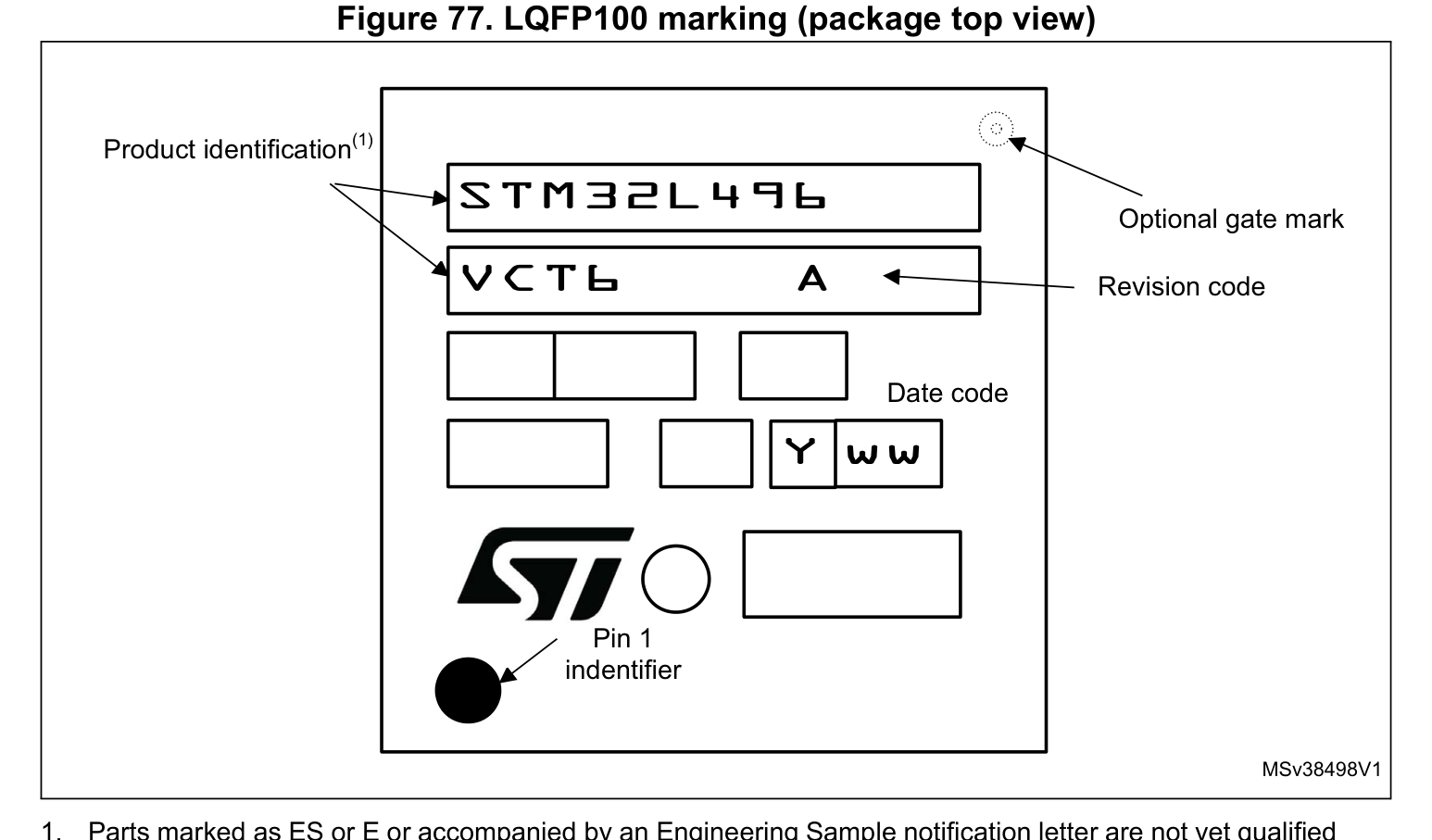
STM32L496VET6 (LQFP-100(14x14)) — Figure 77. LQFP100 marking (package top view)
Figure 77. LQFP100 marking (package top view)
P266 · p266_fig02EXACT PACKAGE
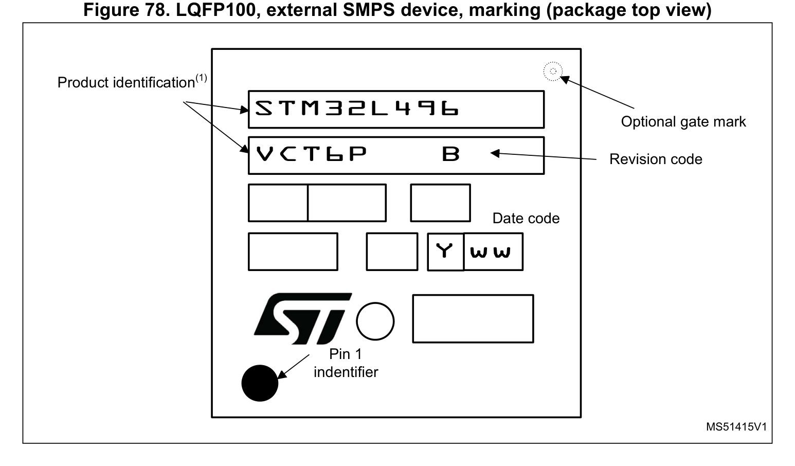
STM32L496VET6 (LQFP-100(14x14)) — Figure 78. LQFP100, external SMPS device, marking (package top view)
Figure 78. LQFP100, external SMPS device, marking (package top view)
P1 · p01_fig01881×421px
STM32L496VET6 (LQFP-100(14x14)) —  Dedicated Chrom-ART Accelerator™ for enhanced graphic content creation (DMA2D)
 Dedicated Chrom-ART Accelerator™ for enhanced graphic content creation (DMA2D)
P66 · p66_fig01P66
STM32L496VET6 (LQFP-100(14x14)) — Datasheet Page 66 (p66_fig01)
Datasheet Page 66 (p66_fig01)
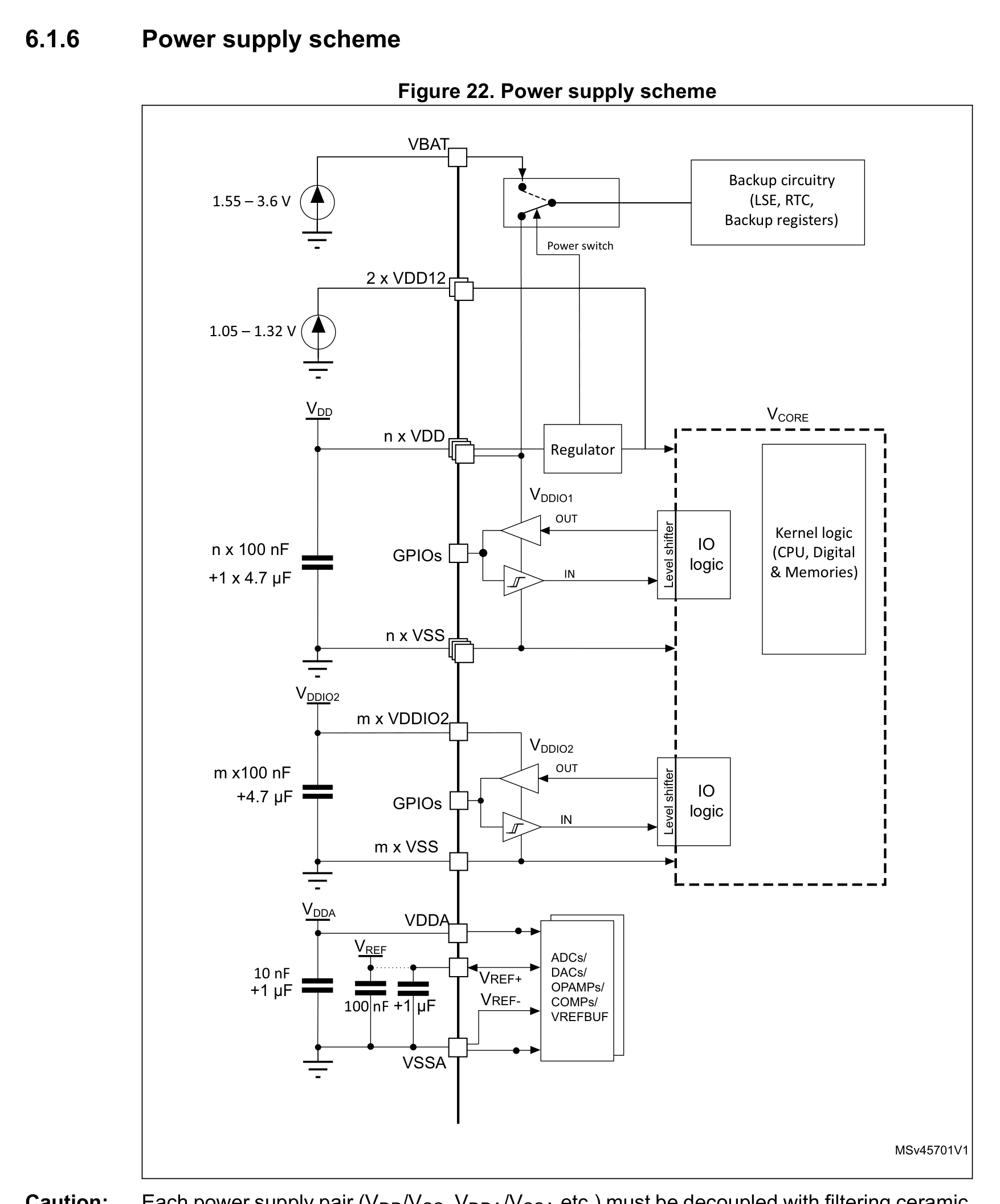
P123 · p123_fig011755×2113px
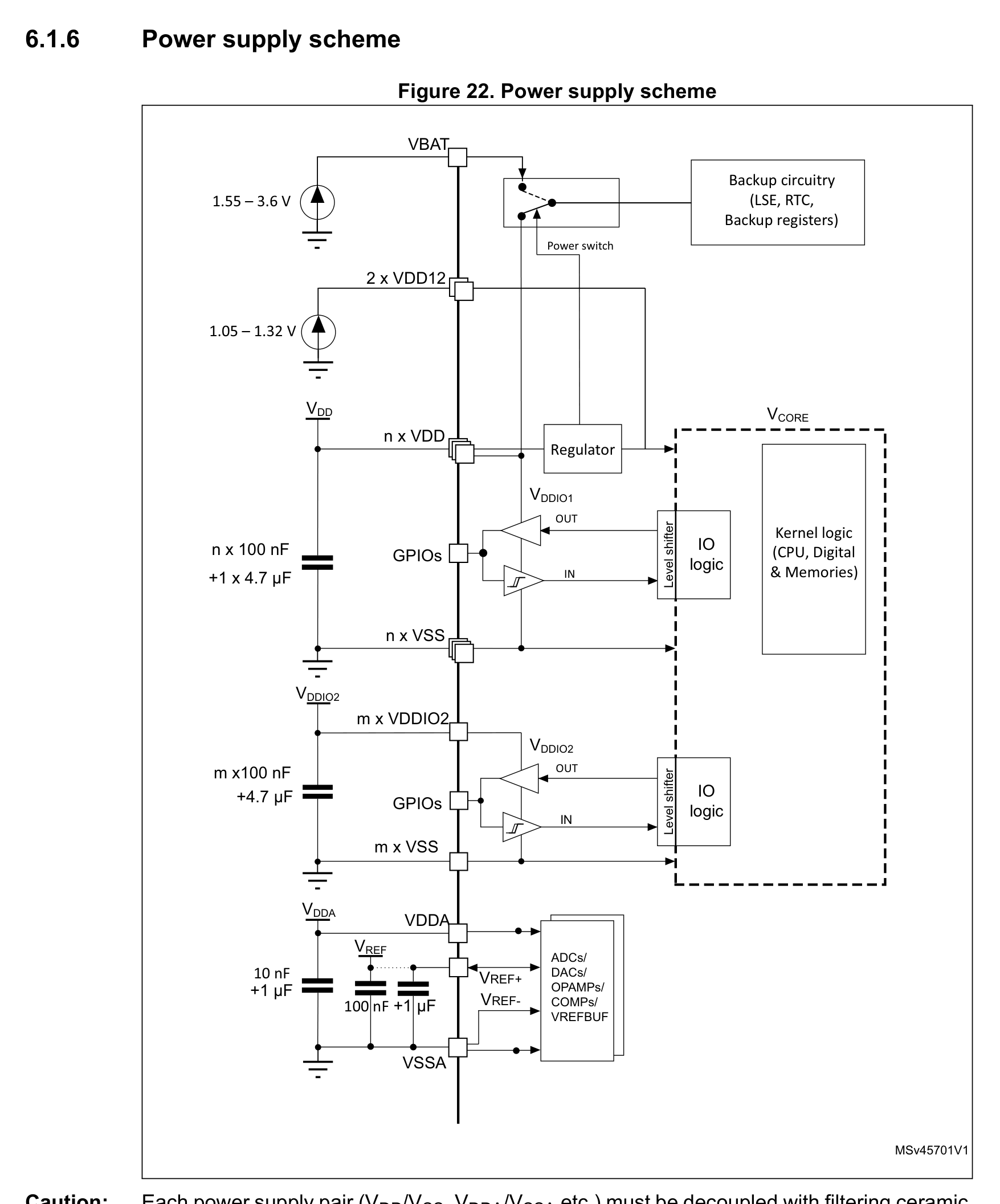
STM32L496VET6 (LQFP-100(14x14)) — Figure 22. Power supply scheme VBAT VBAT
Figure 22. Power supply scheme VBAT VBAT
P123 · p123_fig01P123
STM32L496VET6 (LQFP-100(14x14)) — Datasheet Page 123 (p123_fig01)
Datasheet Page 123 (p123_fig01)
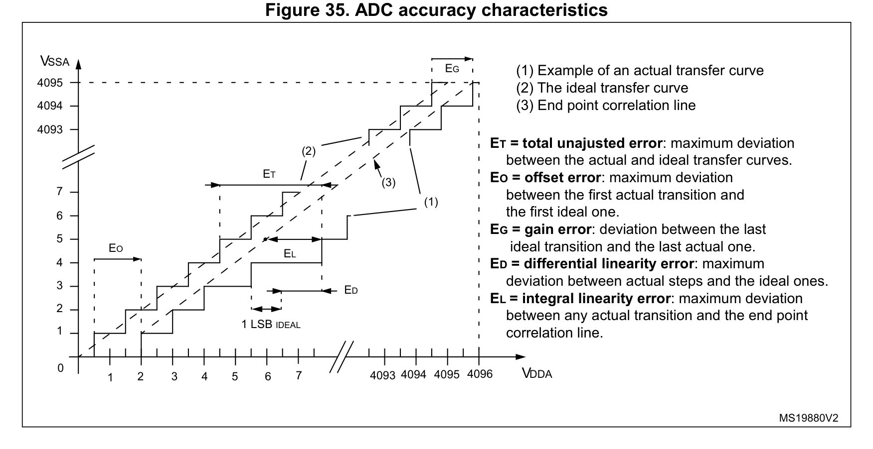
P198 · p198_fig011751×902px
STM32L496VET6 (LQFP-100(14x14)) — Figure 35. ADC accuracy characteristics
Figure 35. ADC accuracy characteristics
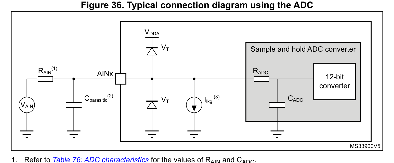
P198 · p198_fig021546×641px
STM32L496VET6 (LQFP-100(14x14)) — Figure 36. Typical connection diagram using the ADC
Figure 36. Typical connection diagram using the ADC
Page 1 / 2 (15 extracted figures)

Technical Specifications & Part Details (STM32L496VET6)

Summary of electrical parameters, mechanical dimensions, voltage range and peripheral interfaces from Datasheet (EN)
Embedded Microcontroller Unit (MCU)
Detailed Overview:STM32L496VET6 (LQFP-100(14x14)) is a 100-pin embedded microcontroller unit (mcu) featuring a 14.00 × 14.00 × 1.60 mm mechanical envelope (lead pitch e = 0.50 mm). Rated for 1.71 V to 3.6 V supply operation across -40°C ~ +85°C (Industrial Grade) with integrated USB, SPI, I2C, ADC, DAC, JTAG / SWD, IrDA, CAN, PWM, RTC/CLK, SWD/JTAG, UART interfaces.
Operating Supply VoltageV_CC / V_DD
1.71 V to 3.6 V
Place 100nF + 10µF X7R decoupling capacitors < 2mm from supply pins
Ambient Operating TemperatureT_A
-40°C ~ +85°C (Industrial Grade)
Industrial temperature grade; T_J(max) = +125°C
Clock / RF Operating Frequencyf_CLK / f_RF
80 MHz
Extracted from authoritative PDF specification tables
Current & Power RatingI_OUT / I_CC
I_GPIO(max) = ±20 mA / pin | I_VDD(total) ≤ 150 mA
79 5V-tolerant (FT) pins detected
Package Envelope (D × E × A)D × E × A
14.00 × 14.00 × 1.60 mm (A1=0.10 mm)
Package family: LQFP (LQFP-100(14x14))
Pin Count & Lead PitchN / e
100 Pins | Pitch e = 0.50 mm (19.7 mil)
Normalized to Center-to-Center Span C per IPC-7351B
Integrated Peripheral InterfacesBuses
USB, SPI, I2C, ADC, DAC, JTAG / SWD, IrDA, CAN, PWM, RTC/CLK, SWD/JTAG, UART
Cross-linked with 4D Pinout & Schematic Symbol
Reflow & Moisture SensitivityIPC / MSL
IPC-7351B Level B | J-STD-020 (Peak 260°C) | MSL-3
60% windowed solder paste stencil on thermal EPAD
Engineering Safety Alert: Boot Strapping Pin Alert (PH3BOOT0 -): Do not force conflicting external pull-ups/pull-downs during POR reset.
Engineering Safety Alert: Connect exposed thermal pad (if present) to internal ground plane via 0.3mm stitched thermal vias.

5-Point Standards Verification

Automated compliance checks prior to export
5/5 PASS
IEEE-315 Symbol100 auto-grouped pins
OK
IPC-7351B Land Pattern100 pads · Pitch 0.50mm
OK
IPC-7525 60% Solder PasteReflow 1:1 Standard
OK
DFM Rules JLCPCB / PCBWayMin pad clearance: 0.25mm
OK
3D STEP AP214 & GLBAligned coordinate origin (0,0,0)
OK

Hardware Verification & Community Engineering Reviews

Summary of electrical parameters, mechanical dimensions, voltage range and peripheral interfaces from Datasheet
5.00 PCB Verified

Mechanical Dimensions & Land Pattern (LQFP-100(14x14))

Extracted from Datasheet & IPC-7351B Normalized
mm
Package Body (D × E)Nominal
14.00 × 14.00 mm
Height (A) & Pitch (e)IPC-7351B
A=1.60mm · e=0.50mm
Pad Size (W × L)Level B
0.30 × 1.20 mm
Pins / Total PadsTopology
100P / 100Pad (QUAD_ROW)

Recommended Companion BOM & Drop-In Equivalents

Passive external components per reference schematic and 1:1 pin-compatible alternatives
DFM READY
Designator / Replacement MPNValue / PackageFunction & PCB Layout Rule
N/A
BOM
Per application circuit
LQFP-100(14x14)
Size power & signal trace widths for rated load current following IPC-2221 clearance rules.

Technical Frequently Asked Questions (FAQ) — STM32L496VET6 (LQFP-100(14x14))

Quick answers covering Pinout, IPC-7351B Land Pattern dimensions, and CAD export formats
IPC-7351B / IEEE-315

What is the Pinout and operating voltage specification of STM32L496VET6 (LQFP-100(14x14))?

Manufactured by ST, the STM32L496VET6 is housed in a LQFP-100(14x14) package with 100 pins and a 0.50 mm lead pitch, supporting a VCC supply range of 1.71 V to 3.6 V. Key pins include: 1 (PE2: Multiplexed I/O & Peripheral Pin PE2 (General)), 2 (PE3: Multiplexed I/O & Peripheral Pin PE3 (General)), 3 (PE4: Multiplexed I/O & Peripheral Pin PE4 (General)), 4 (PE5: Multiplexed I/O & Peripheral Pin PE5 (General)), 5 (PE6: Multiplexed I/O & Peripheral Pin PE6 (I2C, RTC/CLK)), 6 (VBAT: Power Supply Input (VBAT — 3.3V VDD (Max 4.0V))).

What are the IPC-7351B PCB Footprint dimensions for STM32L496VET6?

Normalized from the official datasheet mechanical drawing per IPC-7351B (Density Level B Nominal), STM32L496VET6 (LQFP-100(14x14)) has a nominal body envelope of 14.00 × 14.00 mm, pitch e = 0.50 mm, and 100 copper pads.

Where can I download KiCad (.kicad_mod, .kicad_sym), Fusion 360 (.lbr), and 3D STEP models for STM32L496VET6?

You can download the verified open-hardware (CERN-OHL-P-2.0) CAD library bundle for STM32L496VET6 (ST, LQFP-100(14x14)) directly on this page, including KiCad 8 Footprints (.kicad_mod), Schematic Symbols (.kicad_sym), Autodesk Fusion 360 / Eagle (.lbr), and 3D STEP AP214 / WebGL GLB models.

Static Reference Appendix: Pinout Table (100 pins) & STM32L496 Family VariantsExpand static table
Pin #Signal NameElectrical TypeFunctional Description & Design Notes
1PE2Digital_IOSignal terminal PE2 (I/O, 3.3V VDD (5V-Tolerant FT) domain). Multiplexed alternate functions: PE2. Supported peripheral buses: General.
2PE3Digital_IOSignal terminal PE3 (I/O, 3.3V VDD (5V-Tolerant FT) domain). Multiplexed alternate functions: PE3. Supported peripheral buses: General.
3PE4Digital_IOSignal terminal PE4 (I/O, 3.3V VDD (5V-Tolerant FT) domain). Multiplexed alternate functions: PE4. Supported peripheral buses: General.
4PE5Digital_IOSignal terminal PE5 (I/O, 3.3V VDD (5V-Tolerant FT) domain). Multiplexed alternate functions: PE5. Supported peripheral buses: General.
5PE6Digital_IOSignal terminal PE6 (I/O, 3.3V VDD (5V-Tolerant FT) domain). Multiplexed alternate functions: PE6. Supported peripheral buses: I2C, RTC/CLK.
6VBATPower_InPrimary positive power supply input (VBAT) operating in the 3.3V VDD (Max 4.0V) domain (Max rating: 4.0V).
7PC13Digital_IOSignal terminal PC13 (I/O, 3.3V VDD (5V-Tolerant FT) domain). Multiplexed alternate functions: PC13. Supported peripheral buses: RTC/CLK.
8PC14 - OSC32_IN (PC14)Digital_IOSignal terminal PC14 - OSC32_IN (PC14) (I/O, 3.3V VDD (5V-Tolerant FT) domain). Multiplexed alternate functions: PC14 - OSC32_IN (PC14). Supported peripheral buses: RTC/CLK.
9IO4Digital_IOGPIO4 / RTC_GPIO4 / TOUCH4 / ADC1_CH3
10VSSGND0V electrical ground return terminal (VSS) for internal core logic, I/O drivers, and analog sub-blocks.
11VDDPower_InPrimary positive power supply input (VDD) operating in the 3.3V VDD (Max 4.0V) domain (Max rating: 4.0V).
12PH0OSC IN -_ (PH0)Digital_IOSignal terminal PH0OSC IN -_ (PH0) (I/O, 3.3V VDD (5V-Tolerant FT) domain). Multiplexed alternate functions: PH0OSC IN -_ (PH0). Supported peripheral buses: RTC/CLK.
13PH1 - OSC_OUT (PH1)Digital_IOSignal terminal PH1 - OSC_OUT (PH1) (I/O, 3.3V VDD (5V-Tolerant FT) domain). Multiplexed alternate functions: PH1 - OSC_OUT (PH1). Supported peripheral buses: RTC/CLK.
14NRSTDigital_IOActive-low hardware reset terminal (NRST): pulling this pin Low resets the processor core and peripherals.
15PC0Digital_IOSignal terminal PC0 (I/O, 3.3V VDD (5V-Tolerant FT) domain). Multiplexed alternate functions: I2C3_SCL. Supported peripheral buses: I2C, ADC.
16PC1Digital_IOSignal terminal PC1 (I/O, 3.3V VDD (5V-Tolerant FT) domain). Multiplexed alternate functions: I2C3_SDA. Supported peripheral buses: I2C, ADC.
17PC2Digital_IOSignal terminal PC2 (I/O, 3.3V VDD (5V-Tolerant FT) domain). Multiplexed alternate functions: SPI2_MISO. Supported peripheral buses: SPI, ADC.
18PC3Digital_IOSignal terminal PC3 (I/O, 3.3V VDD (5V-Tolerant FT) domain). Multiplexed alternate functions: SPI2_MOSI. Supported peripheral buses: SPI, ADC.
19VSSA/VREF -GND0V electrical ground return terminal (VSSA/VREF -) for internal core logic, I/O drivers, and analog sub-blocks.
20VREF -AnalogSignal terminal VREF - (Analog, 3.3V VDD (Max 4.0V) domain). Multiplexed alternate functions: VREF -. Supported peripheral buses: General.
21VREF+AnalogSignal terminal VREF+ (Analog, 3.3V VDD (Max 4.0V) domain). Multiplexed alternate functions: VREF+. Supported peripheral buses: General.
22VDDAPower_InPrimary positive power supply input (VDDA) operating in the 3.3V VDD (Max 4.0V) domain (Max rating: 4.0V).
23PA0Digital_IOSignal terminal PA0 (I/O, 3.3V VDD (5V-Tolerant FT) domain). Multiplexed alternate functions: PA0. Supported peripheral buses: UART, ADC, PWM, RTC/CLK.
24PA1Digital_IOSignal terminal PA1 (I/O, 3.3V VDD (5V-Tolerant FT) domain). Multiplexed alternate functions: PA1. Supported peripheral buses: UART, I2C, ADC, PWM.
25PA2Digital_IOSignal terminal PA2 (I/O, 3.3V VDD (5V-Tolerant FT) domain). Multiplexed alternate functions: PA2. Supported peripheral buses: UART, ADC, PWM.
26PA3Digital_IOSignal terminal PA3 (I/O, 3.3V VDD (Max 4.0V) domain). Multiplexed alternate functions: PA3. Supported peripheral buses: UART, ADC, PWM.
27VSSGND0V electrical ground return terminal (VSS) for internal core logic, I/O drivers, and analog sub-blocks.
28VDDPower_InPrimary positive power supply input (VDD) operating in the 3.3V VDD (Max 4.0V) domain (Max rating: 4.0V).
29PA4Digital_IOSignal terminal PA4 (I/O, 3.3V VDD (Max 4.0V) domain). Multiplexed alternate functions: SPI1_NSSSPI3NSS. Supported peripheral buses: UART, SPI, ADC, DAC.
30PA5Digital_IOSignal terminal PA5 (I/O, 3.3V VDD (Max 4.0V) domain). Multiplexed alternate functions: PA5. Supported peripheral buses: ADC, DAC, PWM.
31PA6Digital_IOSignal terminal PA6 (I/O, 3.3V VDD (5V-Tolerant FT) domain). Multiplexed alternate functions: SPI1_MISO. Supported peripheral buses: UART, SPI, ADC.
32PA7Digital_IOSignal terminal PA7 (I/O, 3.3V VDD (5V-Tolerant FT) domain). Multiplexed alternate functions: SPI1_MOSI. Supported peripheral buses: SPI, ADC, PWM.
33PC4Digital_IOSignal terminal PC4 (I/O, 3.3V VDD (5V-Tolerant FT) domain). Multiplexed alternate functions: PC4. Supported peripheral buses: UART, ADC.
34PC5Digital_IOSignal terminal PC5 (I/O, 3.3V VDD (5V-Tolerant FT) domain). Multiplexed alternate functions: PC5. Supported peripheral buses: UART, ADC.
35PB0Digital_IOSignal terminal PB0 (I/O, 3.3V VDD (Max 4.0V) domain). Multiplexed alternate functions: PB0. Supported peripheral buses: UART, ADC, PWM.
36PB1Digital_IOSignal terminal PB1 (I/O, 3.3V VDD (5V-Tolerant FT) domain). Multiplexed alternate functions: PB1. Supported peripheral buses: UART, ADC, PWM.
37PB2Digital_IOSignal terminal PB2 (I/O, 3.3V VDD (5V-Tolerant FT) domain). Multiplexed alternate functions: I2C3_SMBA. Supported peripheral buses: I2C, RTC/CLK.
38PE7Digital_IOSignal terminal PE7 (I/O, 3.3V VDD (5V-Tolerant FT) domain). Multiplexed alternate functions: PE7. Supported peripheral buses: General.
39PE8Digital_IOSignal terminal PE8 (I/O, 3.3V VDD (5V-Tolerant FT) domain). Multiplexed alternate functions: PE8. Supported peripheral buses: PWM.
40PE9Digital_IOSignal terminal PE9 (I/O, 3.3V VDD (5V-Tolerant FT) domain). Multiplexed alternate functions: PE9. Supported peripheral buses: PWM.
41PE10Digital_IOSignal terminal PE10 (I/O, 3.3V VDD (5V-Tolerant FT) domain). Multiplexed alternate functions: PE10. Supported peripheral buses: PWM.
42PE11Digital_IOSignal terminal PE11 (I/O, 3.3V VDD (5V-Tolerant FT) domain). Multiplexed alternate functions: PE11. Supported peripheral buses: PWM.
43PE12Digital_IOSignal terminal PE12 (I/O, 3.3V VDD (5V-Tolerant FT) domain). Multiplexed alternate functions: PE12. Supported peripheral buses: PWM.
44PE13Digital_IOSignal terminal PE13 (I/O, 3.3V VDD (5V-Tolerant FT) domain). Multiplexed alternate functions: PE13. Supported peripheral buses: PWM.
45PE14Digital_IOSignal terminal PE14 (I/O, 3.3V VDD (5V-Tolerant FT) domain). Multiplexed alternate functions: SPI1_MISO. Supported peripheral buses: SPI, PWM.
46PE15Digital_IOSignal terminal PE15 (I/O, 3.3V VDD (5V-Tolerant FT) domain). Multiplexed alternate functions: SPI1_MOSI. Supported peripheral buses: SPI.
47PB10Digital_IOSignal terminal PB10 (I/O, 3.3V VDD (5V-Tolerant FT) domain). Multiplexed alternate functions: PB10. Supported peripheral buses: UART, SPI, I2C, PWM.
48PB11Digital_IOSignal terminal PB11 (I/O, 3.3V VDD (5V-Tolerant FT) domain). Multiplexed alternate functions: I2C2_SDA. Supported peripheral buses: UART, I2C, PWM.
49VSSGNDBottom exposed die attach pad (VSS) providing primary thermal conduction path to the PCB and low-inductance 0V ground return.
50VDDPower_InPrimary positive power supply input (VDD) operating in the 3.3V VDD (Max 4.0V) domain (Max rating: 4.0V).
51PB12Digital_IOSignal terminal PB12 (I/O, 3.3V VDD (5V-Tolerant FT) domain). Multiplexed alternate functions: PB12. Supported peripheral buses: UART, I2C, CAN.
52PB13Digital_IOSignal terminal PB13 (I/O, 3.3V VDD (5V-Tolerant FT) domain). Multiplexed alternate functions: SPI2_SCK. Supported peripheral buses: UART, SPI, PWM.
53PB14Digital_IOSignal terminal PB14 (I/O, 3.3V VDD (5V-Tolerant FT) domain). Multiplexed alternate functions: SPI2_MISO. Supported peripheral buses: UART, SPI, PWM.
54PB15Digital_IOSignal terminal PB15 (I/O, 3.3V VDD (5V-Tolerant FT) domain). Multiplexed alternate functions: SPI2_MOSI. Supported peripheral buses: SPI, I2C, PWM, RTC/CLK.
55PD8Digital_IOSignal terminal PD8 (I/O, 3.3V VDD (5V-Tolerant FT) domain). Multiplexed alternate functions: PD8. Supported peripheral buses: UART.
56PD9Digital_IOSignal terminal PD9 (I/O, 3.3V VDD (5V-Tolerant FT) domain). Multiplexed alternate functions: PD9. Supported peripheral buses: UART.
57PD10Digital_IOSignal terminal PD10 (I/O, 3.3V VDD (5V-Tolerant FT) domain). Multiplexed alternate functions: PD10. Supported peripheral buses: UART, SPI.
58PD11Digital_IOSignal terminal PD11 (I/O, 3.3V VDD (5V-Tolerant FT) domain). Multiplexed alternate functions: I2C4_SMBA. Supported peripheral buses: UART, I2C.
59PD12Digital_IOSignal terminal PD12 (I/O, 3.3V VDD (5V-Tolerant FT) domain). Multiplexed alternate functions: PD12. Supported peripheral buses: UART, PWM.
60PD13Digital_IOSignal terminal PD13 (I/O, 3.3V VDD (5V-Tolerant FT) domain). Multiplexed alternate functions: PD13. Supported peripheral buses: PWM.
61PD14Digital_IOSignal terminal PD14 (I/O, 3.3V VDD (5V-Tolerant FT) domain). Multiplexed alternate functions: PD14. Supported peripheral buses: PWM.
62PD15Digital_IOSignal terminal PD15 (I/O, 3.3V VDD (5V-Tolerant FT) domain). Multiplexed alternate functions: PD15. Supported peripheral buses: PWM.
63PC6Digital_IOSignal terminal PC6 (I/O, 3.3V VDD (5V-Tolerant FT) domain). Multiplexed alternate functions: PC6. Supported peripheral buses: PWM.
64PC7Digital_IOSignal terminal PC7 (I/O, 3.3V VDD (5V-Tolerant FT) domain). Multiplexed alternate functions: PC7. Supported peripheral buses: PWM.