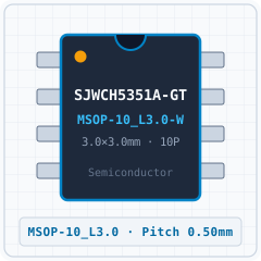
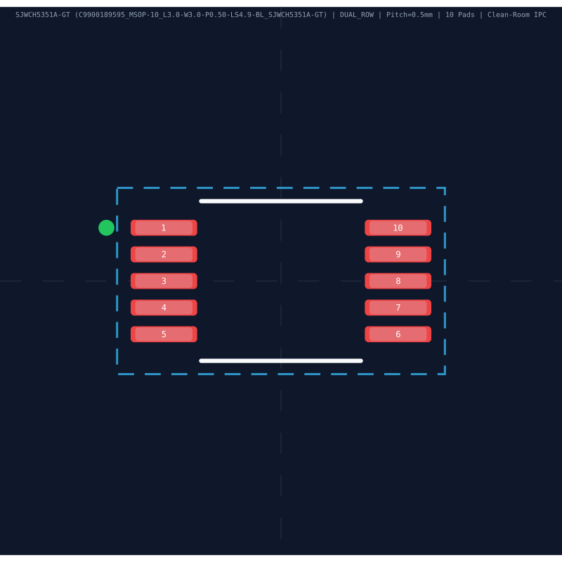
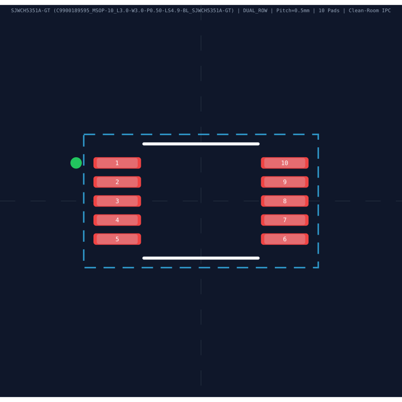
Mechanical Dimensions & Land Pattern (MSOP-10_L3.0-W3.0-P0.50-LS4.9-BL_SJWCH5351A-GT)
Extracted from Datasheet & IPC-7351B NormalizedRecommended Companion BOM & Drop-In Equivalents
Passive external components per reference schematic and 1:1 pin-compatible alternatives| Designator / Replacement MPN | Value / Package | Function & PCB Layout Rule |
|---|---|---|
| N/A BOM | Per application circuit MSOP-10_L3.0-W3.0-P0.50-LS4.9-BL_SJWCH5351A-GT | Size power & signal trace widths for rated load current following IPC-2221 clearance rules. |
Technical Frequently Asked Questions (FAQ) — SJWCH5351A-GT (MSOP-10_L3.0-W3.0-P0.50-LS4.9-BL_SJWCH5351A-GT)
Quick answers covering Pinout, IPC-7351B Land Pattern dimensions, and CAD export formatsWhat is the Pinout and operating voltage specification of SJWCH5351A-GT (MSOP-10_L3.0-W3.0-P0.50-LS4.9-BL_SJWCH5351A-GT)?
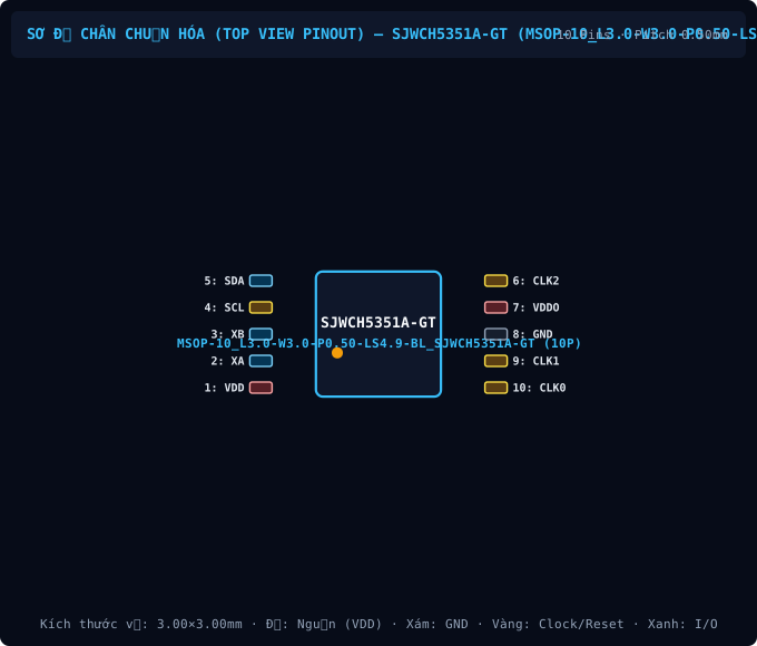
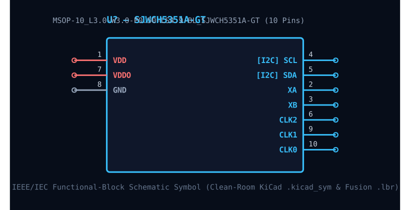
Manufactured by Semiconductor, the SJWCH5351A-GT is housed in a MSOP-10_L3.0-W3.0-P0.50-LS4.9-BL_SJWCH5351A-GT package with 10 pins and a 0.50 mm lead pitch. Key pins include: 1 (VDD: Power Supply Input (VDD — 3.3V / 5.0V Standard Logic)), 2 (XA: Multiplexed I/O & Peripheral Pin XA (General)), 3 (XB: Multiplexed I/O & Peripheral Pin XB (General)), 4 (SCL: Multiplexed I/O & Peripheral Pin SCL (I2C)), 5 (SDA: Multiplexed I/O & Peripheral Pin SDA (I2C)), 6 (CLK2: Multiplexed I/O & Peripheral Pin CLK2 (General)).
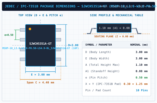
What are the IPC-7351B PCB Footprint dimensions for SJWCH5351A-GT?
Normalized from the official datasheet mechanical drawing per IPC-7351B (Density Level B Nominal), SJWCH5351A-GT (MSOP-10_L3.0-W3.0-P0.50-LS4.9-BL_SJWCH5351A-GT) has a nominal body envelope of 3.00 × 3.00 mm, pitch e = 0.50 mm, and 10 copper pads.
Where can I download KiCad (.kicad_mod, .kicad_sym), Fusion 360 (.lbr), and 3D STEP models for SJWCH5351A-GT?
You can download the verified open-hardware (CERN-OHL-P-2.0) CAD library bundle for SJWCH5351A-GT (Semiconductor, MSOP-10_L3.0-W3.0-P0.50-LS4.9-BL_SJWCH5351A-GT) directly on this page, including KiCad 8 Footprints (.kicad_mod), Schematic Symbols (.kicad_sym), Autodesk Fusion 360 / Eagle (.lbr), and 3D STEP AP214 / WebGL GLB models.
Static Reference Appendix: Pinout Table (10 pins) & C9900189595 Family VariantsExpand static table
| Pin # | Signal Name | Electrical Type | Functional Description & Design Notes |
|---|---|---|---|
| 1 | VDD | Power_In | Primary positive power supply input (VDD) operating in the 3.3V / 5.0V Standard Logic domain (Max rating: 5.5V). |
| 2 | XA | Digital_IO | Signal terminal XA (I/O, 3.3V / 5.0V Standard Logic domain). Multiplexed alternate functions: XA. Supported peripheral buses: General. |
| 3 | XB | Digital_IO | Signal terminal XB (I/O, 3.3V / 5.0V Standard Logic domain). Multiplexed alternate functions: XB. Supported peripheral buses: General. |
| 4 | SCL | Digital_IO | Signal terminal SCL (I/O, 3.3V / 5.0V Standard Logic domain). Multiplexed alternate functions: SCL. Supported peripheral buses: I2C. |
| 5 | SDA | Digital_IO | Signal terminal SDA (I/O, 3.3V / 5.0V Standard Logic domain). Multiplexed alternate functions: SDA. Supported peripheral buses: I2C. |
| 6 | CLK2 | Digital_IO | Signal terminal CLK2 (I/O, 3.3V / 5.0V Standard Logic domain). Multiplexed alternate functions: CLK2. Supported peripheral buses: General. |
| 7 | VDDO | Power_In | Primary positive power supply input (VDDO) operating in the 3.3V / 5.0V Standard Logic domain (Max rating: 5.5V). |
| 8 | GND | GND | 0V electrical ground return terminal (GND) for internal core logic, I/O drivers, and analog sub-blocks. |
| 9 | CLK1 | Digital_IO | Signal terminal CLK1 (I/O, 3.3V / 5.0V Standard Logic domain). Multiplexed alternate functions: CLK1. Supported peripheral buses: General. |
| 10 | CLK0 | Digital_IO | Signal terminal CLK0 (I/O, 3.3V / 5.0V Standard Logic domain). Multiplexed alternate functions: CLK0. Supported peripheral buses: General. |