

PIC24EP256GU810T-I/BG (TFBGA-121) — Symbol, Footprint IPC-7351B & 3D STEP Model

PIC24EP256GU810T-I/BG

MICROCHIPTFBGA-121 · 121 Pins · Pitch 0.80mmIPC-7351B Verified5.0 (0)
SYNCHRONIZED 4D CROSS-PROBE MODETouch or hover any pin to highlight concurrently across Symbol, Footprint and 3D
1. SYMBOL
U1 · PIC24EP256GU810T-I/BG (TFBGA-121)A1IOA1A2IOA2A3RP125/RG13A4IOA4A5RP112/RG0A6VCMPST2/RP97A7VDDA8NoA9RPI76/RD12A10DPH/RP66/RD2A11VCPCON/RP65/B1NoB2RP127/RG15B3IOB3B4IOB4B5AN23/RPI23/RB6VCMPST1/RP96B7VCAPB8PMRD/RP69/RDB9PMBE/RP67/RDB10VSSB11IOB11C1IOC1C2VDDC3RPI124/RG12C4RP126/RG14C5AN22/RPI22/RC6NoC7IOC7C8PMWR/RP68/RDC9NoC10IOC10C11PMCS1/RPI75/D1AN16/PWM5L/RD2IOD2D3IOD3D4NoD5NoD6NoD7C3IN2-/RP70/D8RPI77/RD13D9INT0/DMH/RP6D10NoD11IOD11E1AN19/PWM6H/RE2AN18/PWM6L/RE3IOE3E4AN17/PWM5H/RE5NoE6RP113/RG1E7NoE8RPI31/RA15E9RTCC/DMLN/RPE10IOE10E11RPI30/RA14F1MCLRF2IOF2F3C2IN1-/PMA2/F4IOF4F5VSSF6NoL11SCL2(3)/PMA8L10SDA2(3)/PMA9L9RPI78/RD14L8AN15/PMA0/RPL7AN13/PMA10/RL6RP109/RF13L5IOL5L4AN9/PMA7//RPL3AVSSL2VREF-/RA9L1PGEC1/AN6/RPK11RP98/RF2K10USBID/RP99/RK9RP79/RD15K8VDDK7AN14/PMA1/RPK6RP108/RF12K5NoK4AN8/PMA6/RPIK3VREF+/RA10K2PGED3/AN0/RPK1PGEC3/AN1/RPJ11D-/RG3(5)J10RP104/RF8J9NoJ8NoJ7AN12/PMA11/RJ6TCK/RPI17/RAJ5AN11/PMA12/RJ4AVDDJ3IOJ3J2IOJ2J1IOJ1H11ASCL2(3)/RPIH10D+/RG2(4)H9VUSB3V3H8VBUSH7NoH6VDDH5NoH4NoH3NoH2IOH2H1IOH1G11TDI/RPI20/RAG10ASDA2(3)/RPIG9TDO/RPI21/RAG8NoG7VSSG6VSSG5VDDG4NoG3TMS/RPI16/RAG2AN21/RPI89/RG1AN20/RPI88/RF11OSC2/CLKO/RCF10VSSF9OSC1/RPI60/RF8VDDF7NoGrid Pitch = 2.54mm (IEEE-315)-20.3-15.2-10.2-5.105.110.215.220.383.878.773.768.663.558.453.348.343.238.133.027.922.917.812.77.62.5-2.5-7.6-12.7-17.8-22.9-27.9-33.0-38.1-43.2-48.3-53.3-58.4-63.5-68.6-73.7-78.7-83.8mm
2. 2D FOOTPRINT
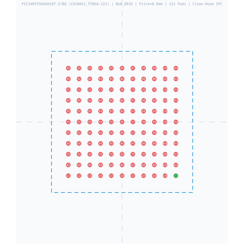
L11K11J11H11G11F11E11D11C11B11A11L10K10J10H10G10F10E10D10C10B10A10L9K9J9H9G9F9E9D9C9B9A9L8K8J8H8G8F8E8D8C8B8A8L7K7J7H7G7F7E7D7C7B7A7L6K6J6H6G6F6E6D6C6B6A6L5K5J5H5G5F5E5D5C5B5A5L4K4J4H4G4F4E4D4C4B4A4L3K3J3H3G3F3E3D3C3B3A3L2K2J2H2G2F2E2D2C2B2A2L1K1J1H1G1F1E1D1C1B1A1E=10.00mm · Pitch e=0.80mmD=10.00mm-7-5-3-113577531-1-3-5-7mm
3. 3D CAD MODEL
Package Body: 10.00mm × 10.00mm · Pitch: 0.80mm · Ruler Step: 1.00mmSynced <100ms

Synchronized Pinout (Symbol / 2D / 3D) (121/121)

Touch or hover any pin to highlight concurrently across Symbol, Footprint and 3D
PinSymbolTypeFunction (EN)
A1IOA1I/OGeneral Purpose Digital I/O Pin IOA1
A2IOA2I/OGeneral Purpose Digital I/O Pin IOA2
A3RP125/RG13I/OMultiplexed I/O & Peripheral Pin RP125/RG13 (General)
A4IOA4I/OGeneral Purpose Digital I/O Pin IOA4
A5RP112/RG0I/OMultiplexed I/O & Peripheral Pin RP112/RG0 (General)
A6VCMPST2/RP97/RF1I/OMultiplexed I/O & Peripheral Pin VCMPST2/RP97/RF1 (General)
A7VDDPowerPower Supply Input (VDD — 3.0V to 3.6V)
A8NoI/OMultiplexed I/O & Peripheral Pin No (General)
A9RPI76/RD12I/OMultiplexed I/O & Peripheral Pin RPI76/RD12 (General)
A10DPH/RP66/RD2I/OMultiplexed I/O & Peripheral Pin DPH/RP66/RD2 (General)
A11VCPCON/RP65/RD1I/OMultiplexed I/O & Peripheral Pin VCPCON/RP65/RD1 (General)
B1NoI/OMultiplexed I/O & Peripheral Pin No (General)
B2RP127/RG15I/OMultiplexed I/O & Peripheral Pin RP127/RG15 (General)
B3IOB3I/OGeneral Purpose Digital I/O Pin IOB3
B4IOB4I/OGeneral Purpose Digital I/O Pin IOB4
B5AN23/RPI23/RA7I/OMultiplexed I/O & Peripheral Pin AN23/RPI23/RA7 (General)
B6VCMPST1/RP96/RF0I/OMultiplexed I/O & Peripheral Pin VCMPST1/RP96/RF0 (General)
B7VCAPI/OMultiplexed I/O & Peripheral Pin VCAP (General)
B8PMRD/RP69/RD5I/OMultiplexed I/O & Peripheral Pin PMRD/RP69/RD5 (General)
B9PMBE/RP67/RD3I/OMultiplexed I/O & Peripheral Pin PMBE/RP67/RD3 (General)
B10VSSGNDGround Reference Pin (VSS)
B11IOB11I/OGeneral Purpose Digital I/O Pin IOB11
C1IOC1I/OGeneral Purpose Digital I/O Pin IOC1
C2VDDPowerPower Supply Input (VDD — 3.0V to 3.6V)
C3RPI124/RG12I/OMultiplexed I/O & Peripheral Pin RPI124/RG12 (General)
C4RP126/RG14I/OMultiplexed I/O & Peripheral Pin RP126/RG14 (General)
C5AN22/RPI22/RA6I/OMultiplexed I/O & Peripheral Pin AN22/RPI22/RA6 (General)
C6NoI/OMultiplexed I/O & Peripheral Pin No (General)
C7IOC7I/OGeneral Purpose Digital I/O Pin IOC7
C8PMWR/RP68/RD4I/OMultiplexed I/O & Peripheral Pin PMWR/RP68/RD4 (General)
C9NoI/OMultiplexed I/O & Peripheral Pin No (General)
C10IOC10I/OGeneral Purpose Digital I/O Pin IOC10
C11PMCS1/RPI75/RD11I/OMultiplexed I/O & Peripheral Pin PMCS1/RPI75/RD11 (General)
D1AN16/PWM5L/RPI49/RC1I/OMultiplexed I/O & Peripheral Pin AN16/PWM5L/RPI49/RC1 (PWM)
D2IOD2I/OGeneral Purpose Digital I/O Pin IOD2
D3IOD3I/OGeneral Purpose Digital I/O Pin IOD3
D4NoI/OMultiplexed I/O & Peripheral Pin No (General)
D5NoI/OMultiplexed I/O & Peripheral Pin No (General)
D6NoI/OMultiplexed I/O & Peripheral Pin No (General)
D7C3IN2-/RP70/RD6I/OMultiplexed I/O & Peripheral Pin C3IN2-/RP70/RD6 (General)
D8RPI77/RD13I/OMultiplexed I/O & Peripheral Pin RPI77/RD13 (General)
D9INT0/DMH/RP64/RD0I/OMultiplexed I/O & Peripheral Pin INT0/DMH/RP64/RD0 (General)
D10NoI/OMultiplexed I/O & Peripheral Pin No (General)
D11IOD11I/OGeneral Purpose Digital I/O Pin IOD11
E1AN19/PWM6H/RPI52/RC4I/OMultiplexed I/O & Peripheral Pin AN19/PWM6H/RPI52/RC4 (PWM)
E2AN18/PWM6L/RPI51/RC3I/OMultiplexed I/O & Peripheral Pin AN18/PWM6L/RPI51/RC3 (PWM)
E3IOE3I/OGeneral Purpose Digital I/O Pin IOE3
E4AN17/PWM5H/RPI50/RC2I/OMultiplexed I/O & Peripheral Pin AN17/PWM5H/RPI50/RC2 (PWM)
E5NoI/OMultiplexed I/O & Peripheral Pin No (General)
E6RP113/RG1I/OMultiplexed I/O & Peripheral Pin RP113/RG1 (General)
E7NoI/OMultiplexed I/O & Peripheral Pin No (General)
E8RPI31/RA15I/OMultiplexed I/O & Peripheral Pin RPI31/RA15 (General)
E9RTCC/DMLN/RPI72/RD8I/OMultiplexed I/O & Peripheral Pin RTCC/DMLN/RPI72/RD8 (RTC/CLK)
E10IOE10I/OGeneral Purpose Digital I/O Pin IOE10
E11RPI30/RA14I/OMultiplexed I/O & Peripheral Pin RPI30/RA14 (General)
F1MCLRI/OMultiplexed I/O & Peripheral Pin MCLR (General)
F2IOF2I/OGeneral Purpose Digital I/O Pin IOF2
F3C2IN1-/PMA2/RPI121/RG9I/OMultiplexed I/O & Peripheral Pin C2IN1-/PMA2/RPI121/RG9 (General)
F4IOF4I/OGeneral Purpose Digital I/O Pin IOF4
F5VSSGNDGround Reference Pin (VSS)
F6NoI/OMultiplexed I/O & Peripheral Pin No (General)
F7NoI/OMultiplexed I/O & Peripheral Pin No (General)
F8VDDPowerPower Supply Input (VDD — 3.0V to 3.6V)
F9OSC1/RPI60/RC12I/OMultiplexed I/O & Peripheral Pin OSC1/RPI60/RC12 (RTC/CLK)
F10VSSGNDGround Reference Pin (VSS)
F11OSC2/CLKO/RC15I/OMultiplexed I/O & Peripheral Pin OSC2/CLKO/RC15 (RTC/CLK)
G1AN20/RPI88/RE8I/OMultiplexed I/O & Peripheral Pin AN20/RPI88/RE8 (General)
G2AN21/RPI89/RE9I/OMultiplexed I/O & Peripheral Pin AN21/RPI89/RE9 (General)
G3TMS/RPI16/RA0I/OMultiplexed I/O & Peripheral Pin TMS/RPI16/RA0 (General)
G4NoI/OMultiplexed I/O & Peripheral Pin No (General)
G5VDDPowerPower Supply Input (VDD — 3.0V to 3.6V)
G6VSSGNDGround Reference Pin (VSS)
G7VSSGNDGround Reference Pin (VSS)
G8NoI/OMultiplexed I/O & Peripheral Pin No (General)
G9TDO/RPI21/RA5I/OMultiplexed I/O & Peripheral Pin TDO/RPI21/RA5 (General)
G10ASDA2(3)/RPI19/RA3I/OMultiplexed I/O & Peripheral Pin ASDA2(3)/RPI19/RA3 (General)
G11TDI/RPI20/RA4I/OMultiplexed I/O & Peripheral Pin TDI/RPI20/RA4 (General)
H1IOH1I/OGeneral Purpose Digital I/O Pin IOH1
H2IOH2I/OGeneral Purpose Digital I/O Pin IOH2
H3NoI/OMultiplexed I/O & Peripheral Pin No (General)
H4NoI/OMultiplexed I/O & Peripheral Pin No (General)
H5NoI/OMultiplexed I/O & Peripheral Pin No (General)
H6VDDPowerPower Supply Input (VDD — 3.0V to 3.6V)
H7NoI/OMultiplexed I/O & Peripheral Pin No (General)
H8VBUSPowerPower Supply Input (VBUS — 3.0V to 3.6V)
H9VUSB3V3PowerPower Supply Input (VUSB3V3 — 3.0V to 3.6V)
H10D+/RG2(4)I/OMultiplexed I/O & Peripheral Pin D+/RG2(4) (USB)
H11ASCL2(3)/RPI18/RA2I/OMultiplexed I/O & Peripheral Pin ASCL2(3)/RPI18/RA2 (General)
J1IOJ1I/OGeneral Purpose Digital I/O Pin IOJ1
J2IOJ2I/OGeneral Purpose Digital I/O Pin IOJ2
J3IOJ3I/OGeneral Purpose Digital I/O Pin IOJ3
J4AVDDPowerPower Supply Input (AVDD — 3.0V to 3.6V)
J5AN11/PMA12/RPI43/RB11I/OMultiplexed I/O & Peripheral Pin AN11/PMA12/RPI43/RB11 (General)
J6TCK/RPI17/RA1I/OMultiplexed I/O & Peripheral Pin TCK/RPI17/RA1 (General)
J7AN12/PMA11/RPI44/RB12I/OMultiplexed I/O & Peripheral Pin AN12/PMA11/RPI44/RB12 (General)
J8NoI/OMultiplexed I/O & Peripheral Pin No (General)
J9NoI/OMultiplexed I/O & Peripheral Pin No (General)
J10RP104/RF8I/OMultiplexed I/O & Peripheral Pin RP104/RF8 (General)
J11D-/RG3(5)I/OMultiplexed I/O & Peripheral Pin D-/RG3(5) (USB)
K1PGEC3/AN1/RPI33/RB1I/OMultiplexed I/O & Peripheral Pin PGEC3/AN1/RPI33/RB1 (General)
K2PGED3/AN0/RPI32/RB0I/OMultiplexed I/O & Peripheral Pin PGED3/AN0/RPI32/RB0 (General)
K3VREF+/RA10AnalogMultiplexed I/O & Peripheral Pin VREF+/RA10 (General)
K4AN8/PMA6/RPI40/RB8I/OMultiplexed I/O & Peripheral Pin AN8/PMA6/RPI40/RB8 (General)
K5NoI/OMultiplexed I/O & Peripheral Pin No (General)
K6RP108/RF12I/OMultiplexed I/O & Peripheral Pin RP108/RF12 (General)
K7AN14/PMA1/RPI46/RB14I/OMultiplexed I/O & Peripheral Pin AN14/PMA1/RPI46/RB14 (General)
K8VDDPowerPower Supply Input (VDD — 3.0V to 3.6V)
K9RP79/RD15I/OMultiplexed I/O & Peripheral Pin RP79/RD15 (General)
K10USBID/RP99/RF3I/OMultiplexed I/O & Peripheral Pin USBID/RP99/RF3 (USB)
K11RP98/RF2I/OMultiplexed I/O & Peripheral Pin RP98/RF2 (General)
L1PGEC1/AN6/RPI38/RB6I/OMultiplexed I/O & Peripheral Pin PGEC1/AN6/RPI38/RB6 (General)
L2VREF-/RA9AnalogMultiplexed I/O & Peripheral Pin VREF-/RA9 (General)
L3AVSSGNDGround Reference Pin (AVSS)
L4AN9/PMA7//RPI41/RB9I/OMultiplexed I/O & Peripheral Pin AN9/PMA7//RPI41/RB9 (General)
L5IOL5I/OGeneral Purpose Digital I/O Pin IOL5
L6RP109/RF13I/OMultiplexed I/O & Peripheral Pin RP109/RF13 (General)
L7AN13/PMA10/RPI45/RB13I/OMultiplexed I/O & Peripheral Pin AN13/PMA10/RPI45/RB13 (General)
L8AN15/PMA0/RPI47/RB15I/OMultiplexed I/O & Peripheral Pin AN15/PMA0/RPI47/RB15 (General)
L9RPI78/RD14I/OMultiplexed I/O & Peripheral Pin RPI78/RD14 (General)
L10SDA2(3)/PMA9/RP100/RF4I/OMultiplexed I/O & Peripheral Pin SDA2(3)/PMA9/RP100/RF4 (I2C)
L11SCL2(3)/PMA8/RP101/RF5I/OMultiplexed I/O & Peripheral Pin SCL2(3)/PMA8/RP101/RF5 (I2C)
PIN A1 IOA1
I/O
General Purpose Digital I/O Pin IOA1
Design note: 3.3V logic domain (3.6V absolute max), 40mA max drive current.
IPC-7351B Solder Density & Span C/G/Z Tuner

Extracted Drawings Gallery (6 Standard Drawings + 12 Extracted Figures)

Read the original datasheet PDF directly or click any drawing to view fullscreen
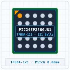
1. Realistic 3D PackageREPRESENTATIVE
PIC24EP256GU810T-I/BG (TFBGA-121) - 1. Realistic 3D Package
Detailed solid 3D bodyExpand ›
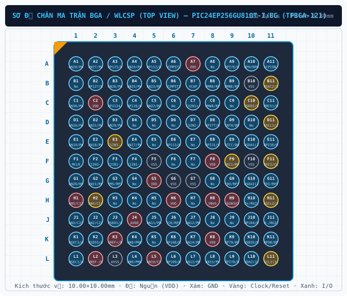
2. Standard Pinout (Top View)CLEANROOM PINOUT
PIC24EP256GU810T-I/BG (TFBGA-121) - 2. Standard Pinout (Top View)
True package pinout (121 pins)Expand ›
3. Original Datasheet PinoutPDF PINOUT
PIC24EP256GU810T-I/BG (TFBGA-121) - 3. Original Datasheet Pinout
Uncropped datasheet pin diagramExpand ›
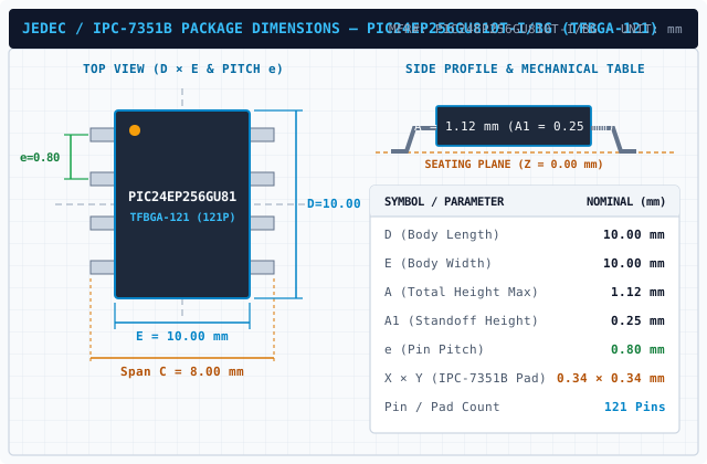
4. Package Dimensions (D×E×A)PACKAGE DIMENSIONS
PIC24EP256GU810T-I/BG (TFBGA-121) - 4. Package Dimensions (D×E×A)
TFBGA-121 · 10.00×10.00mm · Pitch 0.80mmExpand ›
5. Recommended Land PatternLAND PATTERN
PIC24EP256GU810T-I/BG (TFBGA-121) - 5. Recommended Land Pattern
IPC-7351B Footprint (121 Pads)Expand ›
6. Application SchematicSCHEMATIC
PIC24EP256GU810T-I/BG (TFBGA-121) - 6. Application Schematic
Typical Application SchematicExpand ›
Original Datasheet Pinouts & Technical Drawings (12 figures · Page 1/1)
Showing 1–12 of 12 uncropped original figures for PIC24EP256MC / DSPIC33EP512 / DSPIC33EP16G
P1 · p01_fig01377×201px
PIC24EP256GU810T-I/BG (TFBGA-121) — 16-Bit Microcontrollers and Digital Signal Controllers with
16-Bit Microcontrollers and Digital Signal Controllers with
P34 · p34_fig011297×980px
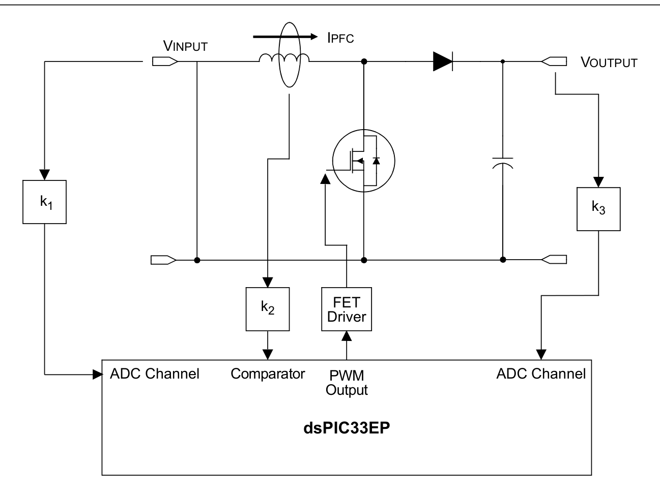
PIC24EP256GU810T-I/BG (TFBGA-121) — FIGURE 2-4: BOOST CONVERTER IMPLEMENTATION
FIGURE 2-4: BOOST CONVERTER IMPLEMENTATION
P36 · p36_fig011469×1006px
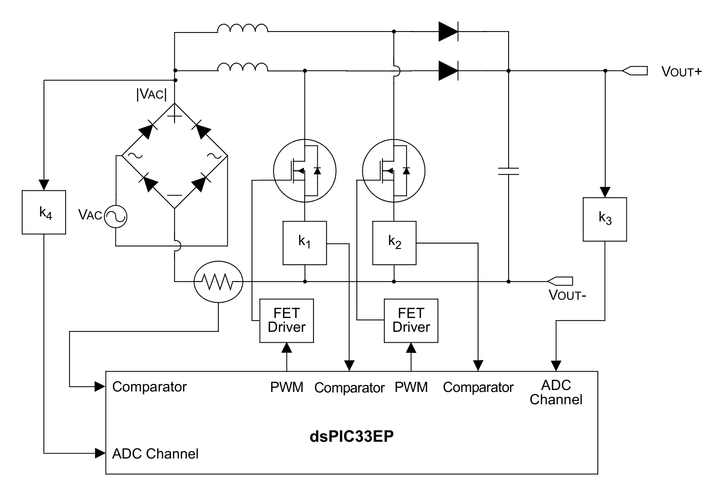
PIC24EP256GU810T-I/BG (TFBGA-121) — FIGURE 2-7: INTERLEAVED PFC
FIGURE 2-7: INTERLEAVED PFC
P36 · p36_fig021162×699px
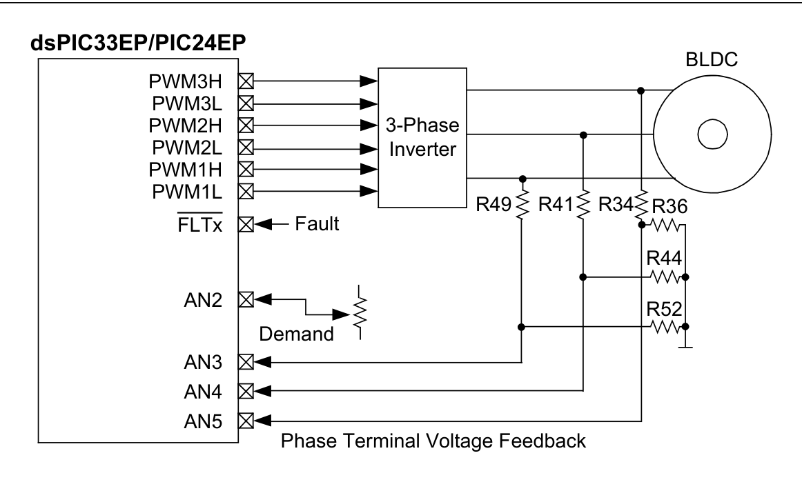
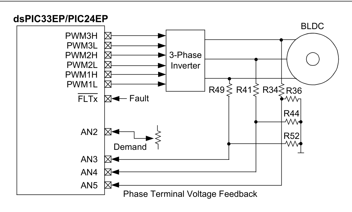
PIC24EP256GU810T-I/BG (TFBGA-121) — FIGURE 2-8: BEMF VOLTAGE MEASURED USING THE ADC MODULE
FIGURE 2-8: BEMF VOLTAGE MEASURED USING THE ADC MODULE
P36 · p36_fig02P36
PIC24EP256GU810T-I/BG (TFBGA-121) — Datasheet Page 36 (p36_fig02)
Datasheet Page 36 (p36_fig02)
P136 · p136_fig01867×545px
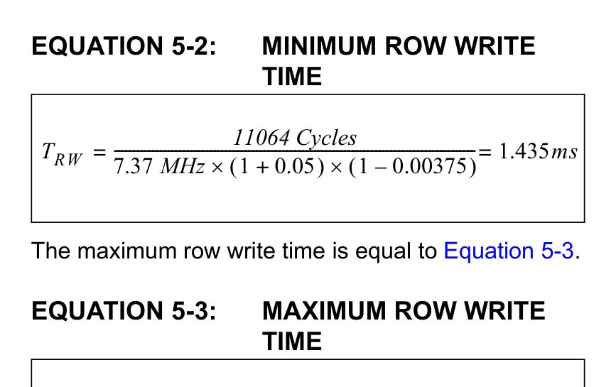
PIC24EP256GU810T-I/BG (TFBGA-121) — TRW 11064 Cycles 7.37 MHz 1 0.05 -   1 0.00375 -     --------------------------------------------------------------------------------------------- 1.586ms = =
TRW 11064 Cycles 7.37 MHz 1 0.05 -   1 0.00375 -     --------------------------------------------------------------------------------------------- 1.586ms = =
P136 · p136_fig02867×440px
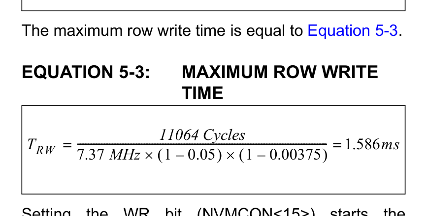
PIC24EP256GU810T-I/BG (TFBGA-121) — The maximum row write time is equal to Equation 5-3. | EQUATION 5-3: MAXIMUM ROW WRITE TIME | Setting the WR bit (NVMCON<15>) starts the operation and the WR bit is automatically cleared when the operation is finished. | TRW 11064 Cycles 7.
The maximum row write time is equal to Equation 5-3. | EQUATION 5-3: MAXIMUM ROW WRITE TIME | Setting the WR bit (NVMCON<15>) starts the operation and the WR bit is automatically cleared when the operation is finished. | TRW 11064 Cycles 7.
P467 · p467_fig011586×924px
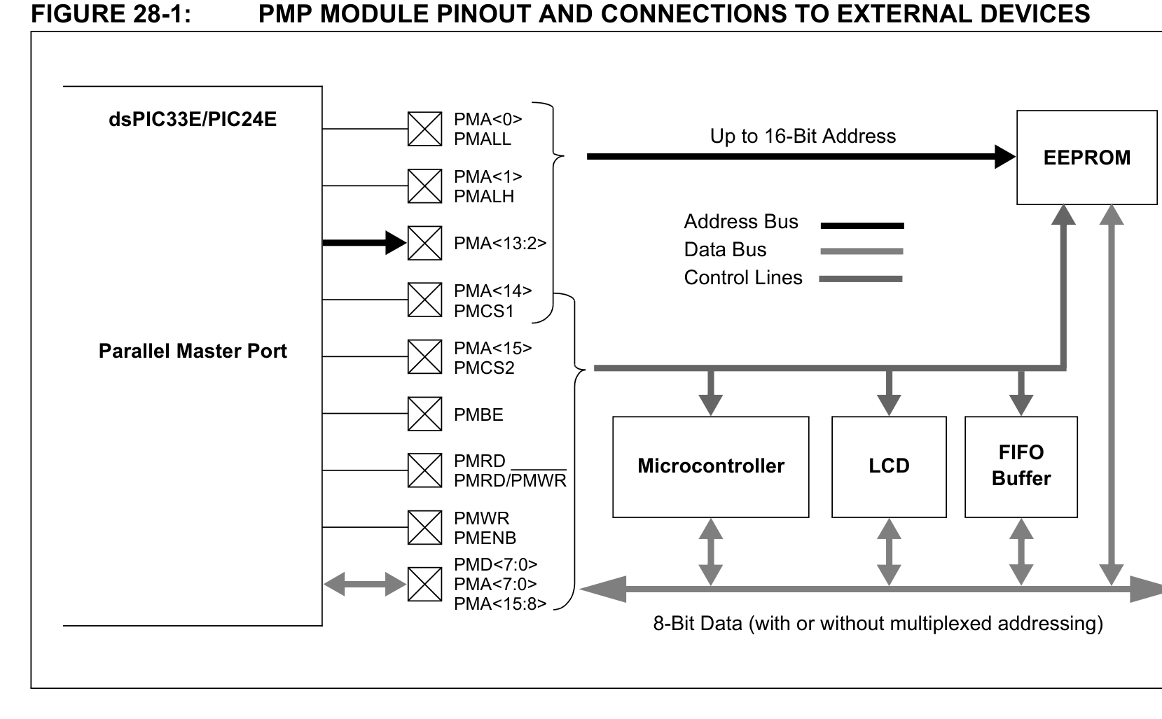
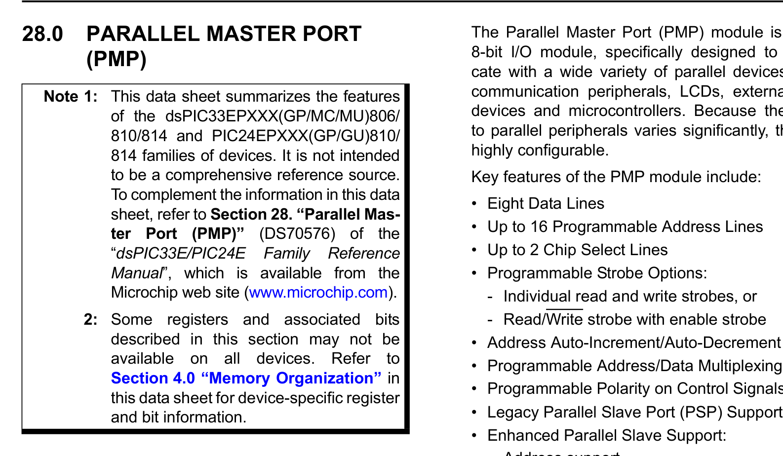
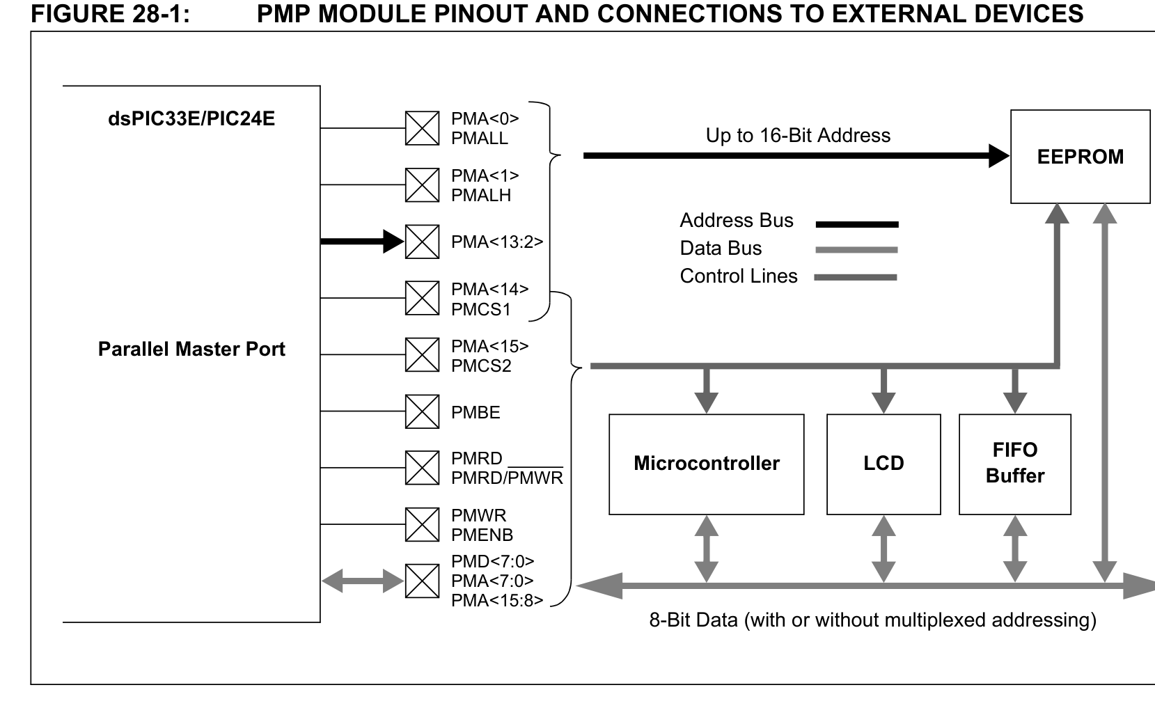
PIC24EP256GU810T-I/BG (TFBGA-121) — FIGURE 28-1: PMP MODULE PINOUT AND CONNECTIONS TO EXTERNAL DEVICES
FIGURE 28-1: PMP MODULE PINOUT AND CONNECTIONS TO EXTERNAL DEVICES
P467 · p467_fig021659×1027px
PIC24EP256GU810T-I/BG (TFBGA-121) — FIGURE 28-1: PMP MODULE PINOUT AND CONNECTIONS TO EXTERNAL DEVICES
FIGURE 28-1: PMP MODULE PINOUT AND CONNECTIONS TO EXTERNAL DEVICES
P467 · p467_fig02P467
PIC24EP256GU810T-I/BG (TFBGA-121) — Datasheet Page 467 (p467_fig02)
Datasheet Page 467 (p467_fig02)
P577 · p577_fig01All Packages in PDF
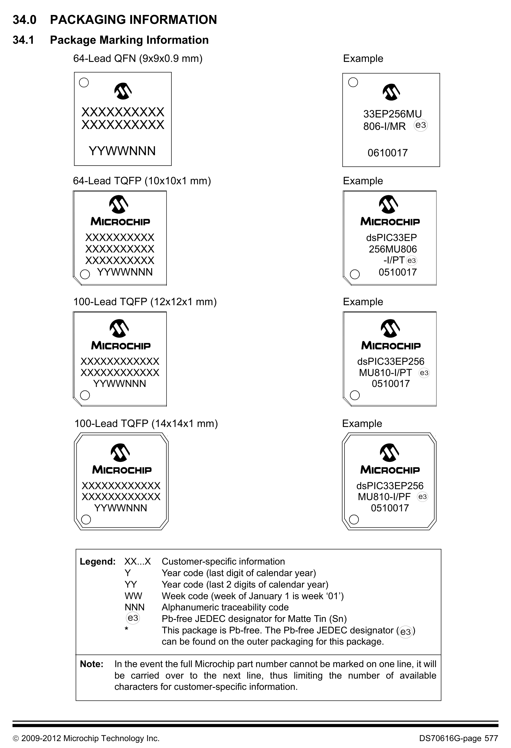
PIC24EP256GU810T-I/BG (TFBGA-121) — dsPIC33EPXXX(GP/MC/MU)806/810/814 and PIC24EPXXX(GP/GU)810/814
dsPIC33EPXXX(GP/MC/MU)806/810/814 and PIC24EPXXX(GP/GU)810/814
P582 · p582_fig01All Packages in PDF
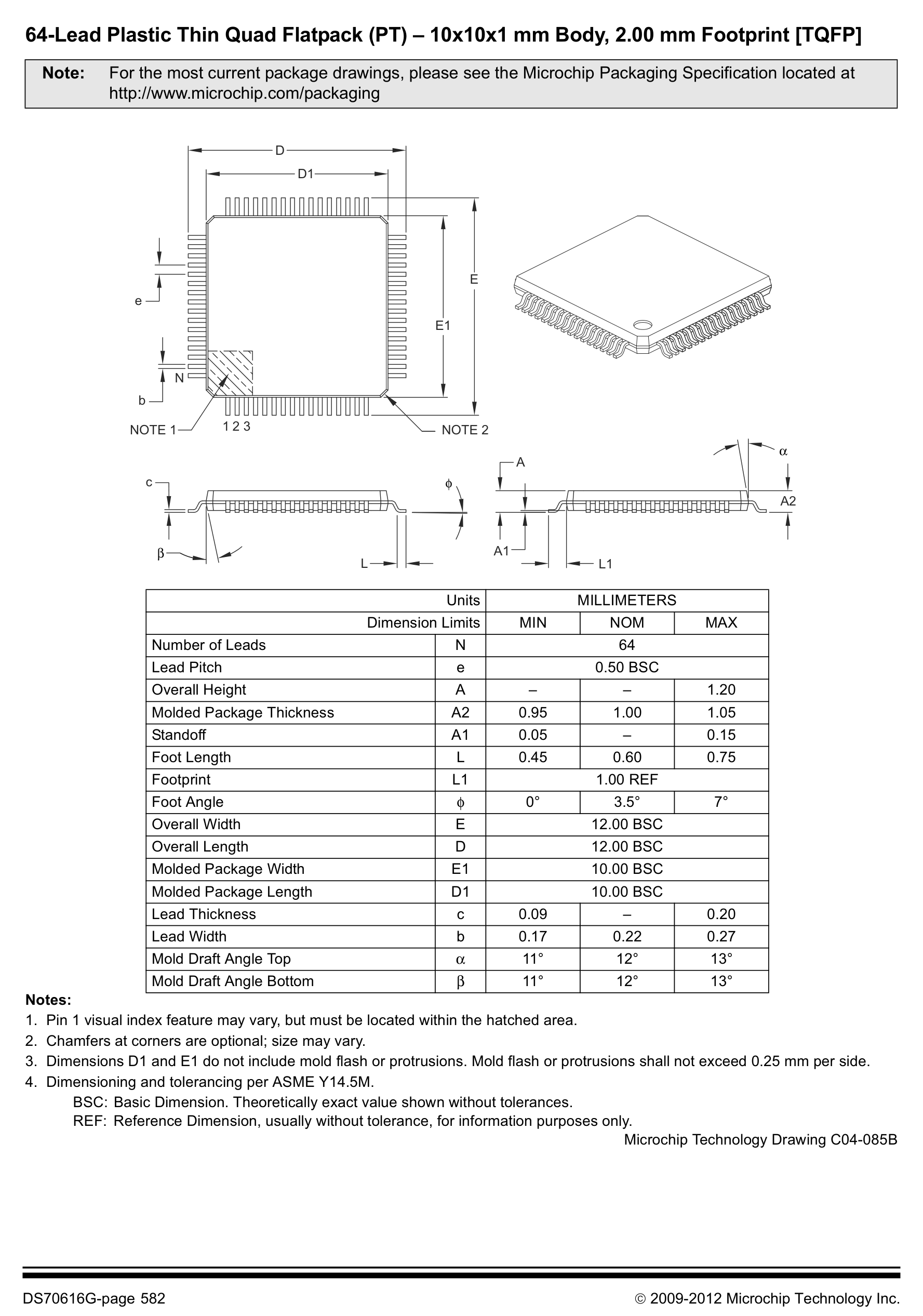
PIC24EP256GU810T-I/BG (TFBGA-121) — DS70616G-page 582  2009-2012 Microchip Technology Inc. | 64-Lead Plastic Thin Quad Flatpack (PT) - 10x10x1 mm Body, 2.00 mm Footprint [TQFP] | Note: For the most current package drawings, please see the Microchip Packaging Specification lo
DS70616G-page 582  2009-2012 Microchip Technology Inc. | 64-Lead Plastic Thin Quad Flatpack (PT) - 10x10x1 mm Body, 2.00 mm Footprint [TQFP] | Note: For the most current package drawings, please see the Microchip Packaging Specification lo

Technical Specifications & Part Details (PIC24EP256GU810T-I/BG)

Summary of electrical parameters, mechanical dimensions, voltage range and peripheral interfaces from Datasheet (EN)
Standard Electronic & Interconnect Component
Detailed Overview:PIC24EP256GU810T-I/BG (TFBGA-121) is a 121-pin standard electronic & interconnect component featuring a 10.00 × 10.00 × 1.12 mm mechanical envelope (lead pitch e = 0.80 mm). Rated for 3.0V to 3.6V supply operation across -40°C to +85°C with integrated USB, UART, SPI, I2C, I2S, ADC, DAC, PWM, JTAG / SWD, IrDA, RTC/CLK interfaces.
Operating Supply VoltageV_CC / V_DD
3.0V to 3.6V
Place 100nF + 10µF X7R decoupling capacitors < 2mm from supply pins
Ambient Operating TemperatureT_A
-40°C to +85°C
Industrial temperature grade; T_J(max) = +125°C
Clock / RF Operating Frequencyf_CLK / f_RF
DC / Broadband Passive
Extracted from authoritative PDF specification tables
Current & Power RatingI_OUT / I_CC
I_GPIO(max) = ±20 mA / pin | I_VDD(total) ≤ 150 mA
Observe per-pin absolute maximum current limits
Package Envelope (D × E × A)D × E × A
10.00 × 10.00 × 1.12 mm (A1=0.25 mm)
Package family: BGA (TFBGA-121)
Pin Count & Lead PitchN / e
121 Pins | Pitch e = 0.80 mm (31.5 mil)
Normalized to Center-to-Center Span C per IPC-7351B
Integrated Peripheral InterfacesBuses
USB, UART, SPI, I2C, I2S, ADC, DAC, PWM, JTAG / SWD, IrDA, RTC/CLK
Cross-linked with 4D Pinout & Schematic Symbol
Reflow & Moisture SensitivityIPC / MSL
IPC-7351B Level B | J-STD-020 (Peak 260°C) | MSL-3
60% windowed solder paste stencil on thermal EPAD
Engineering Safety Alert: Verify Pin-1 chamfer orientation on Top Silkscreen prior to SMT pick-and-place assembly.
Engineering Safety Alert: Connect exposed thermal pad (if present) to internal ground plane via 0.3mm stitched thermal vias.

5-Point Standards Verification

Automated compliance checks prior to export
5/5 PASS
IEEE-315 Symbol121 auto-grouped pins
OK
IPC-7351B Land Pattern121 pads · Pitch 0.80mm
OK
IPC-7525 60% Solder PasteReflow 1:1 Standard
OK
DFM Rules JLCPCB / PCBWayMin pad clearance: 0.25mm
OK
3D STEP AP214 & GLBAligned coordinate origin (0,0,0)
OK

Hardware Verification & Community Engineering Reviews

Summary of electrical parameters, mechanical dimensions, voltage range and peripheral interfaces from Datasheet
5.00 PCB Verified

Mechanical Dimensions & Land Pattern (TFBGA-121)

Extracted from Datasheet & IPC-7351B Normalized
mm
Package Body (D × E)Nominal
10.00 × 10.00 mm
Height (A) & Pitch (e)IPC-7351B
A=1.12mm · e=0.80mm
Pad Size (W × L)Level B
0.34 × 0.34 mm
Pins / Total PadsTopology
121P / 121Pad (BGA_GRID)

Recommended Companion BOM & Drop-In Equivalents

Passive external components per reference schematic and 1:1 pin-compatible alternatives
DFM READY
Designator / Replacement MPNValue / PackageFunction & PCB Layout Rule
N/A
BOM
Per application circuit
TFBGA-121
Size power & signal trace widths for rated load current following IPC-2221 clearance rules.

Technical Frequently Asked Questions (FAQ) — PIC24EP256GU810T-I/BG (TFBGA-121)

Quick answers covering Pinout, IPC-7351B Land Pattern dimensions, and CAD export formats
IPC-7351B / IEEE-315

What is the Pinout and operating voltage specification of PIC24EP256GU810T-I/BG (TFBGA-121)?

Manufactured by MICROCHIP, the PIC24EP256GU810T-I/BG is housed in a TFBGA-121 package with 121 pins and a 0.80 mm lead pitch, supporting a VCC supply range of 3.0V to 3.6V. Key pins include: A1 (IOA1: General Purpose Digital I/O Pin IOA1), A2 (IOA2: General Purpose Digital I/O Pin IOA2), A3 (RP125/RG13: Multiplexed I/O & Peripheral Pin RP125/RG13 (General)), A4 (IOA4: General Purpose Digital I/O Pin IOA4), A5 (RP112/RG0: Multiplexed I/O & Peripheral Pin RP112/RG0 (General)), A6 (VCMPST2/RP97/RF1: Multiplexed I/O & Peripheral Pin VCMPST2/RP97/RF1 (General)).

What are the IPC-7351B PCB Footprint dimensions for PIC24EP256GU810T-I/BG?

Normalized from the official datasheet mechanical drawing per IPC-7351B (Density Level B Nominal), PIC24EP256GU810T-I/BG (TFBGA-121) has a nominal body envelope of 10.00 × 10.00 mm, pitch e = 0.80 mm, and 121 copper pads.

Where can I download KiCad (.kicad_mod, .kicad_sym), Fusion 360 (.lbr), and 3D STEP models for PIC24EP256GU810T-I/BG?

You can download the verified open-hardware (CERN-OHL-P-2.0) CAD library bundle for PIC24EP256GU810T-I/BG (MICROCHIP, TFBGA-121) directly on this page, including KiCad 8 Footprints (.kicad_mod), Schematic Symbols (.kicad_sym), Autodesk Fusion 360 / Eagle (.lbr), and 3D STEP AP214 / WebGL GLB models.

Static Reference Appendix: Pinout Table (121 pins) & PIC24EP256MC / DSPIC33EP512 / DSPIC33EP16G Family VariantsExpand static table
Pin #Signal NameElectrical TypeFunctional Description & Design Notes
A1IOA1Digital_IOGeneral Purpose Digital I/O Pin IOA1
A2IOA2Digital_IOGeneral Purpose Digital I/O Pin IOA2
A3RP125/RG13Digital_IOSignal terminal RP125/RG13 (I/O, 3.0V to 3.6V domain). Multiplexed alternate functions: RP125/RG13. Supported peripheral buses: General.
A4IOA4Digital_IOGeneral Purpose Digital I/O Pin IOA4
A5RP112/RG0Digital_IOSignal terminal RP112/RG0 (I/O, 3.0V to 3.6V domain). Multiplexed alternate functions: RP112/RG0. Supported peripheral buses: General.
A6VCMPST2/RP97/RF1RF_50OhmSignal terminal VCMPST2/RP97/RF1 (I/O, 3.0V to 3.6V domain). Multiplexed alternate functions: VCMPST2/RP97/RF1. Supported peripheral buses: General.
A7VDDPower_InPrimary positive power supply input (VDD) operating in the 3.0V to 3.6V domain (Max rating: 3.6V).
A8NoDigital_IOSignal terminal No (I/O, 3.0V to 3.6V domain). Multiplexed alternate functions: No. Supported peripheral buses: General.
A9RPI76/RD12Digital_IOSignal terminal RPI76/RD12 (I/O, 3.0V to 3.6V domain). Multiplexed alternate functions: RPI76/RD12. Supported peripheral buses: General.
A10DPH/RP66/RD2Digital_IOSignal terminal DPH/RP66/RD2 (I/O, 3.0V to 3.6V domain). Multiplexed alternate functions: DPH/RP66/RD2. Supported peripheral buses: General.
A11VCPCON/RP65/RD1Digital_IOSignal terminal VCPCON/RP65/RD1 (I/O, 3.0V to 3.6V domain). Multiplexed alternate functions: VCPCON/RP65/RD1. Supported peripheral buses: General.
B1NoDigital_IOSignal terminal No (I/O, 3.0V to 3.6V domain). Multiplexed alternate functions: No. Supported peripheral buses: General.
B2RP127/RG15Digital_IOSignal terminal RP127/RG15 (I/O, 3.0V to 3.6V domain). Multiplexed alternate functions: RP127/RG15. Supported peripheral buses: General.
B3IOB3Digital_IOGeneral Purpose Digital I/O Pin IOB3
B4IOB4Digital_IOGeneral Purpose Digital I/O Pin IOB4
B5AN23/RPI23/RA7Digital_IOSignal terminal AN23/RPI23/RA7 (I/O, 3.0V to 3.6V domain). Multiplexed alternate functions: AN23/RPI23/RA7. Supported peripheral buses: General.
B6VCMPST1/RP96/RF0RF_50OhmSignal terminal VCMPST1/RP96/RF0 (I/O, 3.0V to 3.6V domain). Multiplexed alternate functions: VCMPST1/RP96/RF0. Supported peripheral buses: General.
B7VCAPDigital_IOSignal terminal VCAP (I/O, 3.0V to 3.6V domain). Multiplexed alternate functions: VCAP. Supported peripheral buses: General.
B8PMRD/RP69/RD5Digital_IOSignal terminal PMRD/RP69/RD5 (I/O, 3.0V to 3.6V domain). Multiplexed alternate functions: PMRD/RP69/RD5. Supported peripheral buses: General.
B9PMBE/RP67/RD3Digital_IOSignal terminal PMBE/RP67/RD3 (I/O, 3.0V to 3.6V domain). Multiplexed alternate functions: PMBE/RP67/RD3. Supported peripheral buses: General.
B10VSSGND0V electrical ground return terminal (VSS) for internal core logic, I/O drivers, and analog sub-blocks.
B11IOB11Digital_IOGeneral Purpose Digital I/O Pin IOB11
C1IOC1Digital_IOGeneral Purpose Digital I/O Pin IOC1
C2VDDPower_InPrimary positive power supply input (VDD) operating in the 3.0V to 3.6V domain (Max rating: 3.6V).
C3RPI124/RG12Digital_IOSignal terminal RPI124/RG12 (I/O, 3.0V to 3.6V domain). Multiplexed alternate functions: RPI124/RG12. Supported peripheral buses: General.
C4RP126/RG14Digital_IOSignal terminal RP126/RG14 (I/O, 3.0V to 3.6V domain). Multiplexed alternate functions: RP126/RG14. Supported peripheral buses: General.
C5AN22/RPI22/RA6Digital_IOSignal terminal AN22/RPI22/RA6 (I/O, 3.0V to 3.6V domain). Multiplexed alternate functions: AN22/RPI22/RA6. Supported peripheral buses: General.
C6NoDigital_IOSignal terminal No (I/O, 3.0V to 3.6V domain). Multiplexed alternate functions: No. Supported peripheral buses: General.
C7IOC7Digital_IOGeneral Purpose Digital I/O Pin IOC7
C8PMWR/RP68/RD4Digital_IOSignal terminal PMWR/RP68/RD4 (I/O, 3.0V to 3.6V domain). Multiplexed alternate functions: PMWR/RP68/RD4. Supported peripheral buses: General.
C9NoDigital_IOSignal terminal No (I/O, 3.0V to 3.6V domain). Multiplexed alternate functions: No. Supported peripheral buses: General.
C10IOC10Digital_IOGeneral Purpose Digital I/O Pin IOC10
C11PMCS1/RPI75/RD11Digital_IOSignal terminal PMCS1/RPI75/RD11 (I/O, 3.0V to 3.6V domain). Multiplexed alternate functions: PMCS1/RPI75/RD11. Supported peripheral buses: General.
D1AN16/PWM5L/RPI49/RC1Digital_IOSignal terminal AN16/PWM5L/RPI49/RC1 (I/O, 3.0V to 3.6V domain). Multiplexed alternate functions: AN16/PWM5L/RPI49/RC1. Supported peripheral buses: PWM.
D2IOD2Digital_IOGeneral Purpose Digital I/O Pin IOD2
D3IOD3Digital_IOGeneral Purpose Digital I/O Pin IOD3
D4NoDigital_IOSignal terminal No (I/O, 3.0V to 3.6V domain). Multiplexed alternate functions: No. Supported peripheral buses: General.
D5NoDigital_IOSignal terminal No (I/O, 3.0V to 3.6V domain). Multiplexed alternate functions: No. Supported peripheral buses: General.
D6NoDigital_IOSignal terminal No (I/O, 3.0V to 3.6V domain). Multiplexed alternate functions: No. Supported peripheral buses: General.
D7C3IN2-/RP70/RD6Digital_IOSignal terminal C3IN2-/RP70/RD6 (I/O, 3.0V to 3.6V domain). Multiplexed alternate functions: C3IN2-/RP70/RD6. Supported peripheral buses: General.
D8RPI77/RD13Digital_IOSignal terminal RPI77/RD13 (I/O, 3.0V to 3.6V domain). Multiplexed alternate functions: RPI77/RD13. Supported peripheral buses: General.
D9INT0/DMH/RP64/RD0Digital_IOSignal terminal INT0/DMH/RP64/RD0 (I/O, 3.0V to 3.6V domain). Multiplexed alternate functions: INT0/DMH/RP64/RD0. Supported peripheral buses: General.
D10NoDigital_IOSignal terminal No (I/O, 3.0V to 3.6V domain). Multiplexed alternate functions: No. Supported peripheral buses: General.
D11IOD11Digital_IOGeneral Purpose Digital I/O Pin IOD11
E1AN19/PWM6H/RPI52/RC4Digital_IOSignal terminal AN19/PWM6H/RPI52/RC4 (I/O, 3.0V to 3.6V domain). Multiplexed alternate functions: AN19/PWM6H/RPI52/RC4. Supported peripheral buses: PWM.
E2AN18/PWM6L/RPI51/RC3Digital_IOSignal terminal AN18/PWM6L/RPI51/RC3 (I/O, 3.0V to 3.6V domain). Multiplexed alternate functions: AN18/PWM6L/RPI51/RC3. Supported peripheral buses: PWM.
E3IOE3Digital_IOGeneral Purpose Digital I/O Pin IOE3
E4AN17/PWM5H/RPI50/RC2Digital_IOSignal terminal AN17/PWM5H/RPI50/RC2 (I/O, 3.0V to 3.6V domain). Multiplexed alternate functions: AN17/PWM5H/RPI50/RC2. Supported peripheral buses: PWM.
E5NoDigital_IOSignal terminal No (I/O, 3.0V to 3.6V domain). Multiplexed alternate functions: No. Supported peripheral buses: General.
E6RP113/RG1Digital_IOSignal terminal RP113/RG1 (I/O, 3.0V to 3.6V domain). Multiplexed alternate functions: RP113/RG1. Supported peripheral buses: General.
E7NoDigital_IOSignal terminal No (I/O, 3.0V to 3.6V domain). Multiplexed alternate functions: No. Supported peripheral buses: General.
E8RPI31/RA15Digital_IOSignal terminal RPI31/RA15 (I/O, 3.0V to 3.6V domain). Multiplexed alternate functions: RPI31/RA15. Supported peripheral buses: General.
E9RTCC/DMLN/RPI72/RD8Digital_IOSignal terminal RTCC/DMLN/RPI72/RD8 (I/O, 3.0V to 3.6V domain). Multiplexed alternate functions: RTCC/DMLN/RPI72/RD8. Supported peripheral buses: RTC/CLK.
E10IOE10Digital_IOGeneral Purpose Digital I/O Pin IOE10
E11RPI30/RA14Digital_IOSignal terminal RPI30/RA14 (I/O, 3.0V to 3.6V domain). Multiplexed alternate functions: RPI30/RA14. Supported peripheral buses: General.
F1MCLRDigital_IOSignal terminal MCLR (I/O, 3.0V to 3.6V domain). Multiplexed alternate functions: MCLR. Supported peripheral buses: General.
F2IOF2Digital_IOGeneral Purpose Digital I/O Pin IOF2
F3C2IN1-/PMA2/RPI121/RG9Digital_IOSignal terminal C2IN1-/PMA2/RPI121/RG9 (I/O, 3.0V to 3.6V domain). Multiplexed alternate functions: C2IN1-/PMA2/RPI121/RG9. Supported peripheral buses: General.
F4IOF4Digital_IOGeneral Purpose Digital I/O Pin IOF4
F5VSSGND0V electrical ground return terminal (VSS) for internal core logic, I/O drivers, and analog sub-blocks.
F6NoDigital_IOSignal terminal No (I/O, 3.0V to 3.6V domain). Multiplexed alternate functions: No. Supported peripheral buses: General.
F7NoDigital_IOSignal terminal No (I/O, 3.0V to 3.6V domain). Multiplexed alternate functions: No. Supported peripheral buses: General.
F8VDDPower_InPrimary positive power supply input (VDD) operating in the 3.0V to 3.6V domain (Max rating: 3.6V).
F9OSC1/RPI60/RC12Digital_IOSignal terminal OSC1/RPI60/RC12 (I/O, 3.0V to 3.6V domain). Multiplexed alternate functions: OSC1/RPI60/RC12. Supported peripheral buses: RTC/CLK.