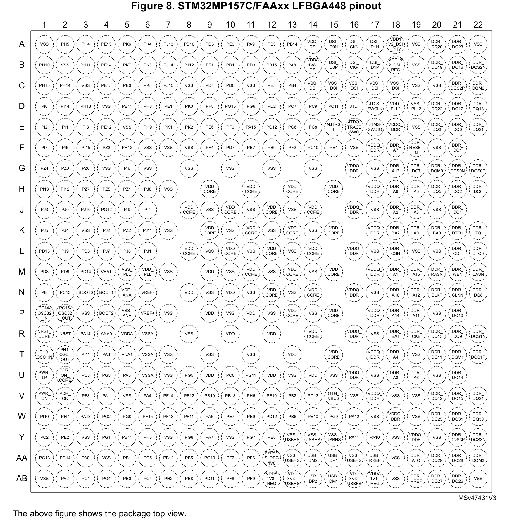
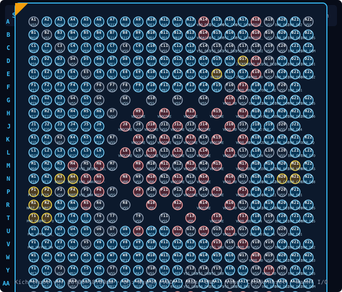
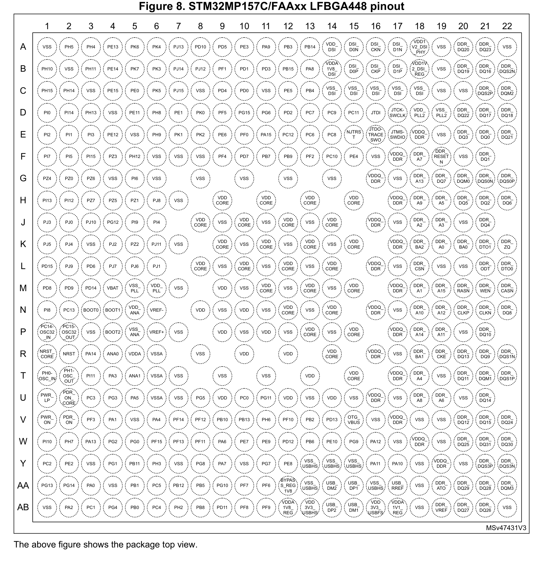
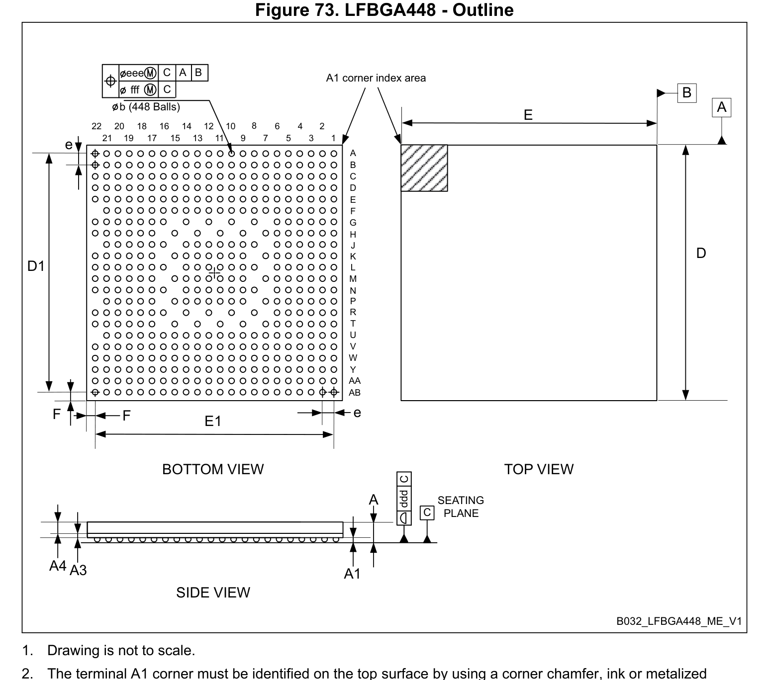
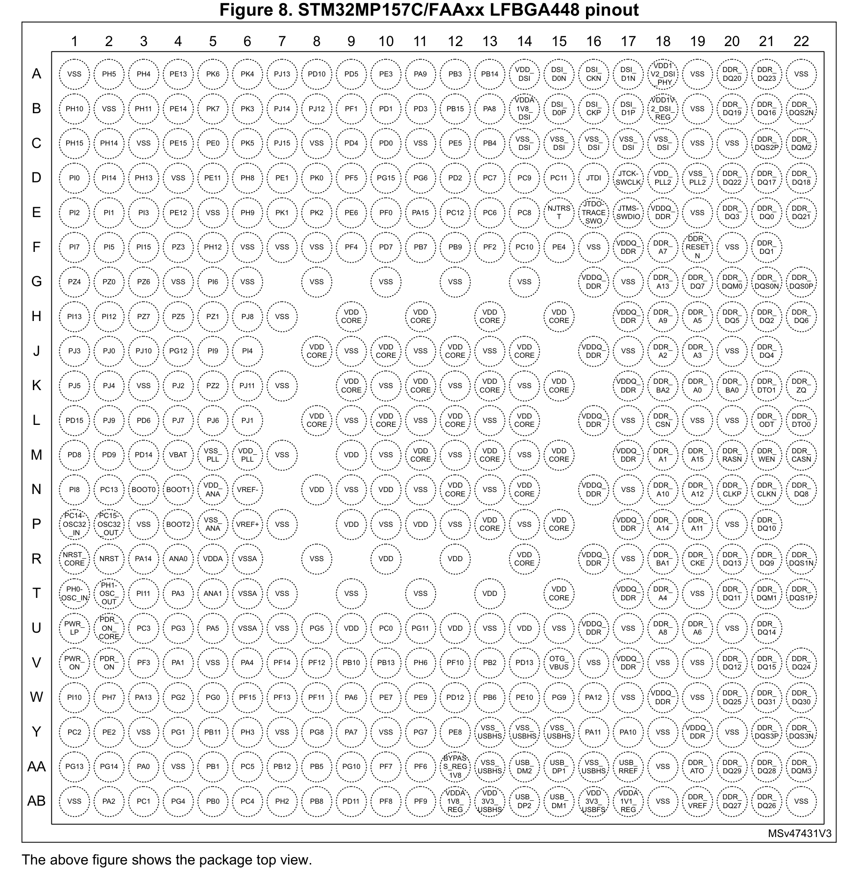
| A1 | VSS | GND | Ground Reference Pin (VSS) |
| A2 | PH5 | I/O | Multiplexed I/O & Peripheral Pin PH5 (I2C) |
| A3 | PH4 | I/O | Multiplexed I/O & Peripheral Pin PH4 (I2C) |
| A4 | PE13 | I/O | Multiplexed I/O & Peripheral Pin PE13 (General) |
| A5 | PK6 | I/O | Multiplexed I/O & Peripheral Pin PK6 (General) |
| A6 | PK4 | I/O | Multiplexed I/O & Peripheral Pin PK4 (General) |
| A7 | PJ13 | I/O | Multiplexed I/O & Peripheral Pin PJ13 (General) |
| A8 | PD10 | I/O | Multiplexed I/O & Peripheral Pin PD10 (SPI, RTC/CLK) |
| A9 | PD5 | I/O | Multiplexed I/O & Peripheral Pin PD5 (UART) |
| A10 | PE3 | I/O | Multiplexed I/O & Peripheral Pin PE3 (General) |
| A11 | PA9 | I/O | Multiplexed I/O & Peripheral Pin PA9 (UART, SPI, PWM) |
| A12 | PB3 | I/O | Multiplexed I/O & Peripheral Pin PB3 (UART, SPI) |
| A13 | PB14 | I/O | Multiplexed I/O & Peripheral Pin PB14 (UART, SPI, PWM) |
| A14 | VDD_DSI | Power | Power Supply Input (VDD_DSI — 3.3V VDD (Max 4.0V)) |
| A15 | DSI_D0N | I/O | Multiplexed I/O & Peripheral Pin DSI_D0N (General) |
| A16 | DSI_CKN | I/O | Multiplexed I/O & Peripheral Pin DSI_CKN (General) |
| A17 | DSI_D1N | I/O | Multiplexed I/O & Peripheral Pin DSI_D1N (General) |
| A18 | VDD1V2_DSI_ PHY | Power | Power Supply Input (VDD1V2_DSI_ PHY — 3.3V VDD (Max 4.0V)) |
| A19 | VSS | GND | Ground Reference Pin (VSS) |
| A20 | DDR_DQ20 | I/O | Multiplexed I/O & Peripheral Pin DDR_DQ20 (General) |
| A21 | DDR_DQ23 | I/O | Multiplexed I/O & Peripheral Pin DDR_DQ23 (General) |
| A22 | VSS | GND | Ground Reference Pin (VSS) |
| B1 | PH10 | I/O | Multiplexed I/O & Peripheral Pin PH10 (I2C, PWM) |
| B2 | VSS | GND | Ground Reference Pin (VSS) |
| B3 | PH11 | I/O | Multiplexed I/O & Peripheral Pin PH11 (I2C, PWM) |
| B4 | PE14 | I/O | Multiplexed I/O & Peripheral Pin PE14 (UART, PWM) |
| B5 | PK7 | I/O | Multiplexed I/O & Peripheral Pin PK7 (General) |
| B6 | PK3 | I/O | Multiplexed I/O & Peripheral Pin PK3 (General) |
| B7 | PJ14 | I/O | Multiplexed I/O & Peripheral Pin PJ14 (General) |
| B8 | PJ12 | I/O | Multiplexed I/O & Peripheral Pin PJ12 (General) |
| B9 | PF1 | I/O | Multiplexed I/O & Peripheral Pin PF1 (I2C) |
| B10 | PD1 | I/O | Multiplexed I/O & Peripheral Pin PD1 (UART, I2C) |
| B11 | PD3 | I/O | Multiplexed I/O & Peripheral Pin PD3 (UART, SPI) |
| B12 | PB15 | I/O | Multiplexed I/O & Peripheral Pin PB15 (UART, SPI, RTC/CLK) |
| B13 | PA8 | I/O | Multiplexed I/O & Peripheral Pin PA8 (UART, SPI, I2C, RTC/CLK) |
| B14 | VDDA1V8_DSI | Power | Power Supply Input (VDDA1V8_DSI — 3.3V VDD (Max 4.0V)) |
| B15 | DSI_D0P | I/O | Multiplexed I/O & Peripheral Pin DSI_D0P (General) |
| B16 | DSI_CKP | I/O | Multiplexed I/O & Peripheral Pin DSI_CKP (General) |
| B17 | DSI_D1P | I/O | Multiplexed I/O & Peripheral Pin DSI_D1P (General) |
| B18 | VDD1V2_DSI_ REG | Power | Power Supply Input (VDD1V2_DSI_ REG — 3.3V VDD (Max 4.0V)) |
| B19 | VSS | GND | Ground Reference Pin (VSS) |
| B20 | DDR_DQ19 | I/O | Multiplexed I/O & Peripheral Pin DDR_DQ19 (General) |
| B21 | DDR_DQ16 | I/O | Multiplexed I/O & Peripheral Pin DDR_DQ16 (General) |
| B22 | DDR_DQS2N | I/O | Multiplexed I/O & Peripheral Pin DDR_DQS2N (General) |
| C1 | PH15 | I/O | Multiplexed I/O & Peripheral Pin PH15 (PWM) |
| C2 | PH14 | I/O | Multiplexed I/O & Peripheral Pin PH14 (UART, PWM) |
| C3 | VSS | GND | Ground Reference Pin (VSS) |
| C4 | PE15 | I/O | Multiplexed I/O & Peripheral Pin PE15 (UART, SPI) |
| C5 | PE0 | I/O | Multiplexed I/O & Peripheral Pin PE0 (SPI) |
| C6 | PK5 | I/O | Multiplexed I/O & Peripheral Pin PK5 (General) |
| C7 | PJ15 | I/O | Multiplexed I/O & Peripheral Pin PJ15 (General) |
| C8 | VSS | GND | Ground Reference Pin (VSS) |
| C9 | PD4 | I/O | Multiplexed I/O & Peripheral Pin PD4 (UART) |
| C10 | PD0 | I/O | Multiplexed I/O & Peripheral Pin PD0 (UART, I2C) |
| C11 | VSS | GND | Ground Reference Pin (VSS) |
| C12 | PE5 | I/O | Multiplexed I/O & Peripheral Pin PE5 (SPI) |
| C13 | PB4 | I/O | Multiplexed I/O & Peripheral Pin PB4 (SPI, PWM) |
| C14 | VSS_DSI | GND | Ground Reference Pin (VSS_DSI) |
| C15 | VSS_DSI | GND | Ground Reference Pin (VSS_DSI) |
| C16 | VSS_DSI | GND | Ground Reference Pin (VSS_DSI) |
| C17 | VSS_DSI | GND | Ground Reference Pin (VSS_DSI) |
| C18 | VSS_DSI | GND | Ground Reference Pin (VSS_DSI) |
| C19 | VSS | GND | Ground Reference Pin (VSS) |
| C20 | VSS | GND | Ground Reference Pin (VSS) |
| C21 | DDR_DQS2P | I/O | Multiplexed I/O & Peripheral Pin DDR_DQS2P (General) |
| C22 | DDR_DQM2 | I/O | Multiplexed I/O & Peripheral Pin DDR_DQM2 (General) |
| D1 | PI0 | I/O | Multiplexed I/O & Peripheral Pin PI0 (SPI) |
| D2 | PI14 | I/O | Multiplexed I/O & Peripheral Pin PI14 (General) |
| D3 | PH13 | I/O | Multiplexed I/O & Peripheral Pin PH13 (PWM) |
| D4 | VSS | GND | Ground Reference Pin (VSS) |
| D5 | PE11 | I/O | Multiplexed I/O & Peripheral Pin PE11 (SPI, PWM) |
| D6 | PH8 | I/O | Multiplexed I/O & Peripheral Pin PH8 (General) |
| D7 | PE1 | I/O | Multiplexed I/O & Peripheral Pin PE1 (General) |
| D8 | PK0 | I/O | Multiplexed I/O & Peripheral Pin PK0 (SPI, PWM) |
| D9 | PF5 | I/O | Multiplexed I/O & Peripheral Pin PF5 (UART) |
| D10 | PG15 | I/O | Multiplexed I/O & Peripheral Pin PG15 (UART, SPI, I2C) |
| D11 | PG6 | I/O | Multiplexed I/O & Peripheral Pin PG6 (General) |
| D12 | PD2 | I/O | Multiplexed I/O & Peripheral Pin PD2 (UART) |
| D13 | PC7 | I/O | Multiplexed I/O & Peripheral Pin PC7 (UART) |
| D14 | PC9 | I/O | Multiplexed I/O & Peripheral Pin PC9 (PWM) |
| D15 | PC11 | I/O | Multiplexed I/O & Peripheral Pin PC11 (UART, SPI) |
| D16 | JTDI | I/O | Multiplexed I/O & Peripheral Pin JTDI (SWD/JTAG) |
| D17 | JTCKSWCLK - | I/O | Multiplexed I/O & Peripheral Pin JTCKSWCLK - (SWD/JTAG) |
| D18 | VDD_PLL2 | Power | Power Supply Input (VDD_PLL2 — 3.3V VDD (Max 4.0V)) |
| D19 | VSS_PLL2 | GND | Ground Reference Pin (VSS_PLL2) |
| D20 | DDR_DQ22 | I/O | Multiplexed I/O & Peripheral Pin DDR_DQ22 (General) |
| D21 | DDR_DQ17 | I/O | Multiplexed I/O & Peripheral Pin DDR_DQ17 (General) |
| D22 | DDR_DQ18 | I/O | Multiplexed I/O & Peripheral Pin DDR_DQ18 (General) |
| E1 | PI2 | I/O | Multiplexed I/O & Peripheral Pin PI2 (SPI, PWM) |
| E2 | PI1 | I/O | Multiplexed I/O & Peripheral Pin PI1 (SPI) |
| E3 | PI3 | I/O | Multiplexed I/O & Peripheral Pin PI3 (SPI) |
| E4 | PE12 | I/O | Multiplexed I/O & Peripheral Pin PE12 (SPI, PWM) |
| E5 | VSS | GND | Ground Reference Pin (VSS) |
| E6 | PH9 | I/O | Multiplexed I/O & Peripheral Pin PH9 (General) |
| E7 | PK1 | I/O | Multiplexed I/O & Peripheral Pin PK1 (PWM) |
| E8 | PK2 | I/O | Multiplexed I/O & Peripheral Pin PK2 (General) |
| E9 | PE6 | I/O | Multiplexed I/O & Peripheral Pin PE6 (SPI) |
| E10 | PF0 | I/O | Multiplexed I/O & Peripheral Pin PF0 (I2C) |
| E11 | PA15 | I/O | Multiplexed I/O & Peripheral Pin PA15 (UART, SPI) |
| E12 | PC12 | I/O | Multiplexed I/O & Peripheral Pin PC12 (UART, SPI, RTC/CLK) |
| E13 | PC6 | I/O | Multiplexed I/O & Peripheral Pin PC6 (UART) |
| E14 | PC8 | I/O | Multiplexed I/O & Peripheral Pin PC8 (UART, PWM) |
| E15 | NJTRST | I/O | Multiplexed I/O & Peripheral Pin NJTRST (SWD/JTAG) |
| E16 | JTDO - TRACESWO | I/O | Multiplexed I/O & Peripheral Pin JTDO - TRACESWO (SWD/JTAG) |
| E17 | JTMS SWDIO - | I/O | Multiplexed I/O & Peripheral Pin JTMS SWDIO - (SWD/JTAG) |
| E18 | VDDQ_DDR | Power | Power Supply Input (VDDQ_DDR — 3.3V VDD (Max 4.0V)) |
| E19 | VSS | GND | Ground Reference Pin (VSS) |
| E20 | DDR_DQ3 | I/O | Multiplexed I/O & Peripheral Pin DDR_DQ3 (General) |
| E21 | DDR_DQ0 | I/O | Multiplexed I/O & Peripheral Pin DDR_DQ0 (General) |
| E22 | DDR_DQ21 | I/O | Multiplexed I/O & Peripheral Pin DDR_DQ21 (General) |
| F1 | PI7 | I/O | Multiplexed I/O & Peripheral Pin PI7 (General) |
| F2 | PI5 | I/O | Multiplexed I/O & Peripheral Pin PI5 (General) |
| F3 | PI15 | I/O | Multiplexed I/O & Peripheral Pin PI15 (General) |
| F4 | PZ3 | I/O | Multiplexed I/O & Peripheral Pin PZ3 (UART, SPI, I2C) |
| F5 | PH12 | I/O | Multiplexed I/O & Peripheral Pin PH12 (I2C) |
| F6 | VSS | GND | Ground Reference Pin (VSS) |
| F7 | VSS | GND | Ground Reference Pin (VSS) |
| F8 | VSS | GND | Ground Reference Pin (VSS) |
| F9 | PF4 | I/O | Multiplexed I/O & Peripheral Pin PF4 (UART) |
| F10 | PD7 | I/O | Multiplexed I/O & Peripheral Pin PD7 (UART, I2C) |
| F11 | PB7 | I/O | Multiplexed I/O & Peripheral Pin PB7 (UART, I2C) |
| F12 | PB9 | I/O | Multiplexed I/O & Peripheral Pin PB9 (SPI) |
| F13 | PF2 | I/O | Multiplexed I/O & Peripheral Pin PF2 (I2C) |
| F14 | PC10 | I/O | Multiplexed I/O & Peripheral Pin PC10 (UART, SPI) |
| F15 | PE4 | I/O | Multiplexed I/O & Peripheral Pin PE4 (SPI) |
| F16 | VSS | GND | Ground Reference Pin (VSS) |
| F17 | VDDQ_DDR | Power | Power Supply Input (VDDQ_DDR — 3.3V VDD (Max 4.0V)) |
| F18 | DDR_A7 | I/O | Multiplexed I/O & Peripheral Pin DDR_A7 (General) |
| F19 | DDR_ RESETN | I | System Enable & Hardware Reset (DDR_ RESETN) |
| F20 | VSS | GND | Ground Reference Pin (VSS) |
| F21 | DDR_DQ1 | I/O | Multiplexed I/O & Peripheral Pin DDR_DQ1 (General) |
| G1 | PZ4 | I/O | Multiplexed I/O & Peripheral Pin PZ4 (I2C) |
| G2 | PZ0 | I/O | Multiplexed I/O & Peripheral Pin PZ0 (UART, SPI, I2C) |
| G3 | PZ6 | I/O | Multiplexed I/O & Peripheral Pin PZ6 (UART, I2C) |
| G4 | VSS | GND | Ground Reference Pin (VSS) |
| G5 | PI6 | I/O | Multiplexed I/O & Peripheral Pin PI6 (General) |
| G6 | VSS | GND | Ground Reference Pin (VSS) |
| G8 | VSS | GND | Ground Reference Pin (VSS) |
| G10 | VSS | GND | Ground Reference Pin (VSS) |
| G12 | VSS | GND | Ground Reference Pin (VSS) |
| G14 | VSS | GND | Ground Reference Pin (VSS) |
| G16 | VDDQ_DDR | Power | Power Supply Input (VDDQ_DDR — 3.3V VDD (Max 4.0V)) |
| G17 | VSS | GND | Ground Reference Pin (VSS) |
| G18 | DDR_A13 | I/O | Multiplexed I/O & Peripheral Pin DDR_A13 (General) |
| G19 | DDR_DQ7 | I/O | Multiplexed I/O & Peripheral Pin DDR_DQ7 (General) |
| G20 | DDR_DQM0 | I/O | Multiplexed I/O & Peripheral Pin DDR_DQM0 (General) |
| G21 | DDR_DQS0N | I/O | Multiplexed I/O & Peripheral Pin DDR_DQS0N (General) |
| G22 | DDR_DQS0P | I/O | Multiplexed I/O & Peripheral Pin DDR_DQS0P (General) |
| H1 | PI13 | I/O | Multiplexed I/O & Peripheral Pin PI13 (General) |
| H2 | PI12 | I/O | Multiplexed I/O & Peripheral Pin PI12 (General) |
| H3 | PZ7 | I/O | Multiplexed I/O & Peripheral Pin PZ7 (UART, I2C) |
| H4 | PZ5 | I/O | Multiplexed I/O & Peripheral Pin PZ5 (UART, I2C) |
| H5 | PZ1 | I/O | Multiplexed I/O & Peripheral Pin PZ1 (SPI, I2C) |
| H6 | PJ8 | I/O | Multiplexed I/O & Peripheral Pin PJ8 (PWM) |
| H7 | VSS | GND | Ground Reference Pin (VSS) |
| H9 | VDDCORE | Power | Power Supply Input (VDDCORE — 3.3V VDD (Max 4.0V)) |
| H11 | VDDCORE | Power | Power Supply Input (VDDCORE — 3.3V VDD (Max 4.0V)) |
| H13 | VDDCORE | Power | Power Supply Input (VDDCORE — 3.3V VDD (Max 4.0V)) |
| H15 | VDDCORE | Power | Power Supply Input (VDDCORE — 3.3V VDD (Max 4.0V)) |
| H17 | VDDQ_DDR | Power | Power Supply Input (VDDQ_DDR — 3.3V VDD (Max 4.0V)) |
| H18 | DDR_A9 | I/O | Multiplexed I/O & Peripheral Pin DDR_A9 (General) |
| H19 | DDR_A5 | I/O | Multiplexed I/O & Peripheral Pin DDR_A5 (General) |
| H20 | DDR_DQ5 | I/O | Multiplexed I/O & Peripheral Pin DDR_DQ5 (General) |
| H21 | DDR_DQ2 | I/O | Multiplexed I/O & Peripheral Pin DDR_DQ2 (General) |
| H22 | DDR_DQ6 | I/O | Multiplexed I/O & Peripheral Pin DDR_DQ6 (General) |
| J1 | PJ3 | I/O | Multiplexed I/O & Peripheral Pin PJ3 (General) |
| J2 | PJ0 | I/O | Multiplexed I/O & Peripheral Pin PJ0 (General) |
| J3 | PJ10 | I/O | Multiplexed I/O & Peripheral Pin PJ10 (SPI, PWM) |
| J4 | PG12 | I/O | Multiplexed I/O & Peripheral Pin PG12 (UART, SPI) |
| J5 | PI9 | I/O | Multiplexed I/O & Peripheral Pin PI9 (UART) |
| J6 | PI4 | I/O | Multiplexed I/O & Peripheral Pin PI4 (General) |
| J8 | VDDCORE | Power | Power Supply Input (VDDCORE — 3.3V VDD (Max 4.0V)) |
| J9 | VSS | GND | Ground Reference Pin (VSS) |
| J10 | VDDCORE | Power | Power Supply Input (VDDCORE — 3.3V VDD (Max 4.0V)) |
| J11 | VSS | GND | Ground Reference Pin (VSS) |
| J12 | VDDCORE | Power | Power Supply Input (VDDCORE — 3.3V VDD (Max 4.0V)) |
| J13 | VSS | GND | Ground Reference Pin (VSS) |
| J14 | VDDCORE | Power | Power Supply Input (VDDCORE — 3.3V VDD (Max 4.0V)) |
| J16 | VDDQ_DDR | Power | Power Supply Input (VDDQ_DDR — 3.3V VDD (Max 4.0V)) |
| J17 | VSS | GND | Ground Reference Pin (VSS) |
| J18 | DDR_A2 | I/O | Multiplexed I/O & Peripheral Pin DDR_A2 (General) |
| J19 | DDR_A3 | I/O | Multiplexed I/O & Peripheral Pin DDR_A3 (General) |
| J20 | VSS | GND | Ground Reference Pin (VSS) |
| J21 | DDR_DQ4 | I/O | Multiplexed I/O & Peripheral Pin DDR_DQ4 (General) |
| K1 | PJ5 | I/O | Multiplexed I/O & Peripheral Pin PJ5 (General) |
| K2 | PJ4 | I/O | Multiplexed I/O & Peripheral Pin PJ4 (General) |
| K3 | VSS | GND | Ground Reference Pin (VSS) |
| K4 | PJ2 | I/O | Multiplexed I/O & Peripheral Pin PJ2 (General) |
| K5 | PZ2 | I/O | Multiplexed I/O & Peripheral Pin PZ2 (SPI, I2C) |
| K6 | PJ11 | I/O | Multiplexed I/O & Peripheral Pin PJ11 (SPI, PWM) |
| K7 | VSS | GND | Ground Reference Pin (VSS) |
| K9 | VDDCORE | Power | Power Supply Input (VDDCORE — 3.3V VDD (Max 4.0V)) |
| K10 | VSS | GND | Ground Reference Pin (VSS) |
| K11 | VDDCORE | Power | Power Supply Input (VDDCORE — 3.3V VDD (Max 4.0V)) |
| K12 | VSS | GND | Ground Reference Pin (VSS) |
| K13 | VDDCORE | Power | Power Supply Input (VDDCORE — 3.3V VDD (Max 4.0V)) |
| K14 | VSS | GND | Ground Reference Pin (VSS) |
| K15 | VDDCORE | Power | Power Supply Input (VDDCORE — 3.3V VDD (Max 4.0V)) |
| K17 | VDDQ_DDR | Power | Power Supply Input (VDDQ_DDR — 3.3V VDD (Max 4.0V)) |
| K18 | DDR_BA2 | I/O | Multiplexed I/O & Peripheral Pin DDR_BA2 (General) |
| K19 | DDR_A0 | I/O | Multiplexed I/O & Peripheral Pin DDR_A0 (General) |
| K20 | DDR_BA0 | I/O | Multiplexed I/O & Peripheral Pin DDR_BA0 (General) |
| K21 | DDR_DTO1 | I/O | Multiplexed I/O & Peripheral Pin DDR_DTO1 (General) |
| K22 | DDR_ZQ | I/O | Multiplexed I/O & Peripheral Pin DDR_ZQ (General) |
| L1 | PD15 | I/O | Multiplexed I/O & Peripheral Pin PD15 (UART) |
| L2 | PJ9 | I/O | Multiplexed I/O & Peripheral Pin PJ9 (PWM) |
| L3 | PD6 | I/O | Multiplexed I/O & Peripheral Pin PD6 (SPI) |
| L4 | PJ7 | I/O | Multiplexed I/O & Peripheral Pin PJ7 (General) |
| L5 | PJ6 | I/O | Multiplexed I/O & Peripheral Pin PJ6 (General) |
| L6 | PJ1 | I/O | Multiplexed I/O & Peripheral Pin PJ1 (General) |
| L8 | VDDCORE | Power | Power Supply Input (VDDCORE — 3.3V VDD (Max 4.0V)) |
| L9 | VSS | GND | Ground Reference Pin (VSS) |
| L10 | VDDCORE | Power | Power Supply Input (VDDCORE — 3.3V VDD (Max 4.0V)) |
| L11 | VSS | GND | Ground Reference Pin (VSS) |
| L12 | VDDCORE | Power | Power Supply Input (VDDCORE — 3.3V VDD (Max 4.0V)) |
| L13 | VSS | GND | Ground Reference Pin (VSS) |
| L14 | VDDCORE | Power | Power Supply Input (VDDCORE — 3.3V VDD (Max 4.0V)) |
| L16 | VDDQ_DDR | Power | Power Supply Input (VDDQ_DDR — 3.3V VDD (Max 4.0V)) |
| L17 | VSS | GND | Ground Reference Pin (VSS) |
| L18 | DDR_CSN | I/O | Multiplexed I/O & Peripheral Pin DDR_CSN (SPI) |
| L19 | VSS | GND | Ground Reference Pin (VSS) |
| L20 | VSS | GND | Ground Reference Pin (VSS) |
| L21 | DDR_ODT | I/O | Multiplexed I/O & Peripheral Pin DDR_ODT (General) |
| L22 | DDR_DTO0 | I/O | Multiplexed I/O & Peripheral Pin DDR_DTO0 (General) |
| M1 | PD8 | I/O | Multiplexed I/O & Peripheral Pin PD8 (UART) |
| M2 | PD9 | I/O | Multiplexed I/O & Peripheral Pin PD9 (UART) |
| M3 | PD14 | I/O | Multiplexed I/O & Peripheral Pin PD14 (UART) |
| M4 | VBAT | Power | Power Supply Input (VBAT — 3.3V VDD (Max 4.0V)) |
| M5 | VSS_PLL | GND | Ground Reference Pin (VSS_PLL) |
| M6 | VDD_PLL | Power | Power Supply Input (VDD_PLL — 3.3V VDD (Max 4.0V)) |
| M7 | VSS | GND | Ground Reference Pin (VSS) |
| M9 | VDD | Power | Power Supply Input (VDD — 3.3V VDD (Max 4.0V)) |
| M10 | VSS | GND | Ground Reference Pin (VSS) |
| M11 | VDDCORE | Power | Power Supply Input (VDDCORE — 3.3V VDD (Max 4.0V)) |
| M12 | VSS | GND | Ground Reference Pin (VSS) |
| M13 | VDDCORE | Power | Power Supply Input (VDDCORE — 3.3V VDD (Max 4.0V)) |
| M14 | VSS | GND | Ground Reference Pin (VSS) |
| M15 | VDDCORE | Power | Power Supply Input (VDDCORE — 3.3V VDD (Max 4.0V)) |
| M17 | VDDQ_DDR | Power | Power Supply Input (VDDQ_DDR — 3.3V VDD (Max 4.0V)) |
| M18 | DDR_A1 | I/O | Multiplexed I/O & Peripheral Pin DDR_A1 (General) |
| M19 | DDR_A15 | I/O | Multiplexed I/O & Peripheral Pin DDR_A15 (General) |
| M20 | DDR_RASN | I/O | Multiplexed I/O & Peripheral Pin DDR_RASN (General) |
| M21 | DDR_WEN | I/O | Multiplexed I/O & Peripheral Pin DDR_WEN (General) |
| M22 | DDR_CASN | I/O | Multiplexed I/O & Peripheral Pin DDR_CASN (General) |
| N1 | PI8 | I/O | Multiplexed I/O & Peripheral Pin PI8 (RTC/CLK) |
| N2 | PC13 | I/O | Multiplexed I/O & Peripheral Pin PC13 (RTC/CLK) |
| N3 | BOOT0 | I | Input-Only Pin BOOT0 (General) |
| N4 | BOOT1 | I/O | Multiplexed I/O & Peripheral Pin BOOT1 (General) |
| N5 | VDD_ANA | Power | Power Supply Input (VDD_ANA — 3.3V VDD (Max 4.0V)) |
| N6 | VREF - | Analog | Multiplexed I/O & Peripheral Pin VREF - (General) |
| N8 | VDD | Power | Power Supply Input (VDD — 3.3V VDD (Max 4.0V)) |
| N9 | VSS | GND | Ground Reference Pin (VSS) |
| N10 | VDD | Power | Power Supply Input (VDD — 3.3V VDD (Max 4.0V)) |
| N11 | VSS | GND | Ground Reference Pin (VSS) |
| N12 | VDDCORE | Power | Power Supply Input (VDDCORE — 3.3V VDD (Max 4.0V)) |
| N13 | VSS | GND | Ground Reference Pin (VSS) |
| N14 | VDDCORE | Power | Power Supply Input (VDDCORE — 3.3V VDD (Max 4.0V)) |
| N16 | VDDQ_DDR | Power | Power Supply Input (VDDQ_DDR — 3.3V VDD (Max 4.0V)) |
| N17 | VSS | GND | Ground Reference Pin (VSS) |
| N18 | DDR_A10 | I/O | Multiplexed I/O & Peripheral Pin DDR_A10 (General) |
| N19 | DDR_A12 | I/O | Multiplexed I/O & Peripheral Pin DDR_A12 (General) |
| N20 | DDR_CLKP | I/O | Multiplexed I/O & Peripheral Pin DDR_CLKP (General) |
| N21 | DDR_CLKN | I/O | Multiplexed I/O & Peripheral Pin DDR_CLKN (General) |
| N22 | DDR_DQ8 | I/O | Multiplexed I/O & Peripheral Pin DDR_DQ8 (General) |
| P1 | PC14 - OSC32_IN | I/O | Multiplexed I/O & Peripheral Pin PC14 - OSC32_IN (RTC/CLK) |
| P2 | PC15 - OSC32_OUT | I/O | Multiplexed I/O & Peripheral Pin PC15 - OSC32_OUT (RTC/CLK) |
| P3 | VSS | GND | Ground Reference Pin (VSS) |
| P4 | BOOT2 | I/O | Multiplexed I/O & Peripheral Pin BOOT2 (General) |
| P5 | VSS_ANA | GND | Ground Reference Pin (VSS_ANA) |
| P6 | VREF+ | Analog | Multiplexed I/O & Peripheral Pin VREF+ (General) |
| P7 | VSS | GND | Ground Reference Pin (VSS) |
| P9 | VDD | Power | Power Supply Input (VDD — 3.3V VDD (Max 4.0V)) |
| P10 | VSS | GND | Ground Reference Pin (VSS) |
| P11 | VDD | Power | Power Supply Input (VDD — 3.3V VDD (Max 4.0V)) |
| P12 | VSS | GND | Ground Reference Pin (VSS) |
| P13 | VDDCORE | Power | Power Supply Input (VDDCORE — 3.3V VDD (Max 4.0V)) |
| P14 | VSS | GND | Ground Reference Pin (VSS) |
| P15 | VDDCORE | Power | Power Supply Input (VDDCORE — 3.3V VDD (Max 4.0V)) |
| P17 | VDDQ_DDR | Power | Power Supply Input (VDDQ_DDR — 3.3V VDD (Max 4.0V)) |
| P18 | DDR_A14 | I/O | Multiplexed I/O & Peripheral Pin DDR_A14 (General) |
| P19 | DDR_A11 | I/O | Multiplexed I/O & Peripheral Pin DDR_A11 (General) |
| P20 | VSS | GND | Ground Reference Pin (VSS) |
| P21 | DDR_DQ10 | I/O | Multiplexed I/O & Peripheral Pin DDR_DQ10 (General) |
| R1 | NRST_CORE | I/O | Multiplexed I/O & Peripheral Pin NRST_CORE (General) |
| R2 | NRST | I | System Enable & Hardware Reset (NRST) |
| R3 | PA14 | I/O | Multiplexed I/O & Peripheral Pin PA14 (RTC/CLK) |
| R4 | ANA0 | I/O | Multiplexed I/O & Peripheral Pin ANA0 (ADC) |
| R5 | VDDA | Power | Power Supply Input (VDDA — 3.3V VDD (Max 4.0V)) |
| R6 | VSSA | GND | Ground Reference Pin (VSSA) |
| R8 | VSS | GND | Ground Reference Pin (VSS) |
| R10 | VDD | Power | Power Supply Input (VDD — 3.3V VDD (Max 4.0V)) |
| R12 | VDD | Power | Power Supply Input (VDD — 3.3V VDD (Max 4.0V)) |
| R14 | VDDCORE | Power | Power Supply Input (VDDCORE — 3.3V VDD (Max 4.0V)) |
| R16 | VDDQ_DDR | Power | Power Supply Input (VDDQ_DDR — 3.3V VDD (Max 4.0V)) |
| R17 | VSS | GND | Ground Reference Pin (VSS) |
| R18 | DDR_BA1 | I/O | Multiplexed I/O & Peripheral Pin DDR_BA1 (General) |
| R19 | DDR_CKE | I/O | Multiplexed I/O & Peripheral Pin DDR_CKE (General) |
| R20 | DDR_DQ13 | I/O | Multiplexed I/O & Peripheral Pin DDR_DQ13 (General) |
| R21 | DDR_DQ9 | I/O | Multiplexed I/O & Peripheral Pin DDR_DQ9 (General) |
| R22 | DDR_DQS1N | I/O | Multiplexed I/O & Peripheral Pin DDR_DQS1N (General) |
| T1 | PH0 OSC IN -_ | I/O | Multiplexed I/O & Peripheral Pin PH0 OSC IN -_ (RTC/CLK) |
| T2 | PH1 - OSC_OUT | I/O | Multiplexed I/O & Peripheral Pin PH1 - OSC_OUT (RTC/CLK) |
| T3 | PI11 | I/O | Multiplexed I/O & Peripheral Pin PI11 (RTC/CLK) |
| T4 | PA3 | I/O | Multiplexed I/O & Peripheral Pin PA3 (UART, ADC, PWM) |
| T5 | ANA1 | I/O | Multiplexed I/O & Peripheral Pin ANA1 (ADC) |
| T6 | VSSA | GND | Ground Reference Pin (VSSA) |
| T7 | VSS | GND | Ground Reference Pin (VSS) |
| T9 | VSS | GND | Ground Reference Pin (VSS) |
| T11 | VSS | GND | Ground Reference Pin (VSS) |
| T13 | VDD | Power | Power Supply Input (VDD — 3.3V VDD (Max 4.0V)) |
| T15 | VDDCORE | Power | Power Supply Input (VDDCORE — 3.3V VDD (Max 4.0V)) |
| T17 | VDDQ_DDR | Power | Power Supply Input (VDDQ_DDR — 3.3V VDD (Max 4.0V)) |
| T18 | DDR_A4 | I/O | Multiplexed I/O & Peripheral Pin DDR_A4 (General) |
| T19 | VSS | GND | Ground Reference Pin (VSS) |
| T20 | DDR_DQ11 | I/O | Multiplexed I/O & Peripheral Pin DDR_DQ11 (General) |
| T21 | DDR_DQM1 | I/O | Multiplexed I/O & Peripheral Pin DDR_DQM1 (General) |
| T22 | DDR_DQS1P | I/O | Multiplexed I/O & Peripheral Pin DDR_DQS1P (General) |
| U1 | PWR_LP | I/O | Multiplexed I/O & Peripheral Pin PWR_LP (General) |
| U2 | PDR_ON_ CORE | I/O | Multiplexed I/O & Peripheral Pin PDR_ON_ CORE (General) |
| U3 | PC3 | I/O | Multiplexed I/O & Peripheral Pin PC3 (SPI, ADC) |
| U4 | PG3 | I/O | Multiplexed I/O & Peripheral Pin PG3 (UART) |
| U5 | PA5 | I/O | Multiplexed I/O & Peripheral Pin PA5 (SPI, ADC, DAC, PWM) |
| U6 | VSSA | GND | Ground Reference Pin (VSSA) |
| U7 | VSS | GND | Ground Reference Pin (VSS) |
| U8 | PG5 | I/O | Multiplexed I/O & Peripheral Pin PG5 (General) |
| U9 | VDD | Power | Power Supply Input (VDD — 3.3V VDD (Max 4.0V)) |
| U10 | PC0 | I/O | Multiplexed I/O & Peripheral Pin PC0 (ADC) |
| U11 | PG11 | I/O | Multiplexed I/O & Peripheral Pin PG11 (UART) |
| U12 | VDD | Power | Power Supply Input (VDD — 3.3V VDD (Max 4.0V)) |
| U13 | VSS | GND | Ground Reference Pin (VSS) |
| U14 | VDD | Power | Power Supply Input (VDD — 3.3V VDD (Max 4.0V)) |
| U15 | VSS | GND | Ground Reference Pin (VSS) |
| U16 | VDDQ_DDR | Power | Power Supply Input (VDDQ_DDR — 3.3V VDD (Max 4.0V)) |
| U17 | VSS | GND | Ground Reference Pin (VSS) |
| U18 | DDR_A8 | I/O | Multiplexed I/O & Peripheral Pin DDR_A8 (General) |
| U19 | DDR_A6 | I/O | Multiplexed I/O & Peripheral Pin DDR_A6 (General) |
| U20 | VSS | GND | Ground Reference Pin (VSS) |
| U21 | DDR_DQ14 | I/O | Multiplexed I/O & Peripheral Pin DDR_DQ14 (General) |
| V1 | PWR_ON | I/O | Multiplexed I/O & Peripheral Pin PWR_ON (General) |
| V2 | PDR_ON | I/O | Multiplexed I/O & Peripheral Pin PDR_ON (General) |
| V3 | PF3 | I/O | Multiplexed I/O & Peripheral Pin PF3 (General) |
| V4 | PA1 | I/O | Multiplexed I/O & Peripheral Pin PA1 (UART, ADC, PWM) |
| V5 | VSS | GND | Ground Reference Pin (VSS) |
| V6 | PA4 | I/O | Multiplexed I/O & Peripheral Pin PA4 (UART, SPI, ADC, DAC) |
| V7 | PF14 | I/O | Multiplexed I/O & Peripheral Pin PF14 (UART, I2C, ADC) |
| V8 | PF12 | I/O | Multiplexed I/O & Peripheral Pin PF12 (UART, ADC) |
| V9 | PB10 | I/O | Multiplexed I/O & Peripheral Pin PB10 (SPI, I2C, PWM) |
| V10 | PB13 | I/O | Multiplexed I/O & Peripheral Pin PB13 (UART, SPI, PWM) |
| V11 | PH6 | I/O | Multiplexed I/O & Peripheral Pin PH6 (UART, SPI) |
| V12 | PF10 | I/O | Multiplexed I/O & Peripheral Pin PF10 (General) |
| V13 | PB2 | I/O | Multiplexed I/O & Peripheral Pin PB2 (UART, SPI, I2C, RTC/CLK) |
| V14 | PD13 | I/O | Multiplexed I/O & Peripheral Pin PD13 (SPI, I2C) |
| V15 | OTG_VBUS | Power | Power Supply Input (OTG_VBUS — 3.3V VDD (5V-Tolerant FT)) |
| V16 | VSS | GND | Ground Reference Pin (VSS) |
| V17 | VDDQ_DDR | Power | Power Supply Input (VDDQ_DDR — 3.3V VDD (Max 4.0V)) |
| V18 | VSS | GND | Ground Reference Pin (VSS) |
| V19 | VSS | GND | Ground Reference Pin (VSS) |
| V20 | DDR_DQ12 | I/O | Multiplexed I/O & Peripheral Pin DDR_DQ12 (General) |
| V21 | DDR_DQ15 | I/O | Multiplexed I/O & Peripheral Pin DDR_DQ15 (General) |
| V22 | DDR_DQ24 | I/O | Multiplexed I/O & Peripheral Pin DDR_DQ24 (General) |
| W1 | PI10 | I/O | Multiplexed I/O & Peripheral Pin PI10 (UART, SPI) |
| W2 | PH7 | I/O | Multiplexed I/O & Peripheral Pin PH7 (UART, I2C) |
| W3 | PA13 | I/O | Multiplexed I/O & Peripheral Pin PA13 (UART, RTC/CLK) |
| W4 | PG2 | I/O | Multiplexed I/O & Peripheral Pin PG2 (UART, RTC/CLK) |
| W5 | PG0 | I/O | Multiplexed I/O & Peripheral Pin PG0 (UART) |
| W6 | PF15 | I/O | Multiplexed I/O & Peripheral Pin PF15 (I2C) |
| W7 | PF13 | I/O | Multiplexed I/O & Peripheral Pin PF13 (UART, I2C, ADC) |
| W8 | PF11 | I/O | Multiplexed I/O & Peripheral Pin PF11 (SPI, ADC) |
| W9 | PA6 | I/O | Multiplexed I/O & Peripheral Pin PA6 (SPI, ADC) |
| W10 | PE7 | I/O | Multiplexed I/O & Peripheral Pin PE7 (General) |
| W11 | PE9 | I/O | Multiplexed I/O & Peripheral Pin PE9 (UART, PWM) |
| W12 | PD12 | I/O | Multiplexed I/O & Peripheral Pin PD12 (UART, I2C) |
| W13 | PB6 | I/O | Multiplexed I/O & Peripheral Pin PB6 (UART, I2C) |
| W14 | PE10 | I/O | Multiplexed I/O & Peripheral Pin PE10 (UART, PWM) |
| W15 | PG9 | I/O | Multiplexed I/O & Peripheral Pin PG9 (UART) |
| W16 | PA12 | I/O | Multiplexed I/O & Peripheral Pin PA12 (UART, I2C) |
| W17 | VSS | GND | Ground Reference Pin (VSS) |
| W18 | VDDQ_DDR | Power | Power Supply Input (VDDQ_DDR — 3.3V VDD (Max 4.0V)) |
| W19 | VSS | GND | Ground Reference Pin (VSS) |
| W20 | DDR_DQ25 | I/O | Multiplexed I/O & Peripheral Pin DDR_DQ25 (General) |
| W21 | DDR_DQ31 | I/O | Multiplexed I/O & Peripheral Pin DDR_DQ31 (General) |
| W22 | DDR_DQ30 | I/O | Multiplexed I/O & Peripheral Pin DDR_DQ30 (General) |
| Y1 | PC2 | I/O | Multiplexed I/O & Peripheral Pin PC2 (UART, SPI, ADC) |
| Y2 | PE2 | I/O | Multiplexed I/O & Peripheral Pin PE2 (UART, I2C) |
| Y3 | VSS | GND | Ground Reference Pin (VSS) |
| Y4 | PG1 | I/O | Multiplexed I/O & Peripheral Pin PG1 (UART) |
| Y5 | PB11 | I/O | Multiplexed I/O & Peripheral Pin PB11 (UART, I2C, PWM) |
| Y6 | PH3 | I/O | Multiplexed I/O & Peripheral Pin PH3 (General) |
| Y7 | VSS | GND | Ground Reference Pin (VSS) |
| Y8 | PG8 | I/O | Multiplexed I/O & Peripheral Pin PG8 (UART, SPI) |
| Y9 | PA7 | I/O | Multiplexed I/O & Peripheral Pin PA7 (SPI, I2C, ADC, PWM) |
| Y10 | VSS | GND | Ground Reference Pin (VSS) |
| Y11 | PG7 | I/O | Multiplexed I/O & Peripheral Pin PG7 (UART) |
| Y12 | PE8 | I/O | Multiplexed I/O & Peripheral Pin PE8 (UART, PWM) |
| Y13 | VSS_USBHS | GND | Ground Reference Pin (VSS_USBHS) |
| Y14 | VSS_USBHS | GND | Ground Reference Pin (VSS_USBHS) |
| Y15 | VSS_USBHS | GND | Ground Reference Pin (VSS_USBHS) |
| Y16 | PA11 | I/O | Multiplexed I/O & Peripheral Pin PA11 (UART, SPI, I2C, PWM) |
| Y17 | PA10 | I/O | Multiplexed I/O & Peripheral Pin PA10 (UART, SPI) |
| Y18 | VSS | GND | Ground Reference Pin (VSS) |
| Y19 | VDDQ_DDR | Power | Power Supply Input (VDDQ_DDR — 3.3V VDD (Max 4.0V)) |
| Y20 | VSS | GND | Ground Reference Pin (VSS) |
| Y21 | DDR_DQS3P | I/O | Multiplexed I/O & Peripheral Pin DDR_DQS3P (General) |
| Y22 | DDR_DQS3N | I/O | Multiplexed I/O & Peripheral Pin DDR_DQS3N (General) |
| AA1 | PG13 | I/O | Multiplexed I/O & Peripheral Pin PG13 (UART, SPI) |
| AA2 | PG14 | I/O | Multiplexed I/O & Peripheral Pin PG14 (UART, SPI) |
| AA3 | PA0 | I/O | Multiplexed I/O & Peripheral Pin PA0 (UART, SPI, ADC, PWM) |
| AA4 | VSS | GND | Ground Reference Pin (VSS) |
| AA5 | PB1 | I/O | Multiplexed I/O & Peripheral Pin PB1 (UART, ADC, PWM) |
| AA6 | PC5 | I/O | Multiplexed I/O & Peripheral Pin PC5 (UART, ADC) |
| AA7 | PB12 | I/O | Multiplexed I/O & Peripheral Pin PB12 (UART, SPI, I2C) |
| AA8 | PB5 | I/O | Multiplexed I/O & Peripheral Pin PB5 (UART, SPI, I2C, PWM) |
| AA9 | PG10 | I/O | Multiplexed I/O & Peripheral Pin PG10 (UART) |
| AA10 | PF7 | I/O | Multiplexed I/O & Peripheral Pin PF7 (General) |
| AA11 | PF6 | I/O | Multiplexed I/O & Peripheral Pin PF6 (SPI) |
| AA12 | BYPASS_ REG1V8 | I/O | Multiplexed I/O & Peripheral Pin BYPASS_ REG1V8 (General) |
| AA13 | VSS_USBHS | GND | Ground Reference Pin (VSS_USBHS) |
| AA14 | USB_DM2 | I/O | Multiplexed I/O & Peripheral Pin USB_DM2 (USB) |
| AA15 | USB_DP1 | I/O | Multiplexed I/O & Peripheral Pin USB_DP1 (USB) |
| AA16 | VSS_USBHS | GND | Ground Reference Pin (VSS_USBHS) |
| AA17 | USB_RREF | I/O | Multiplexed I/O & Peripheral Pin USB_RREF (USB) |
| AA18 | VSS | GND | Ground Reference Pin (VSS) |
| AA19 | DDR_ATO | I/O | Multiplexed I/O & Peripheral Pin DDR_ATO (General) |
| AA20 | DDR_DQ29 | I/O | Multiplexed I/O & Peripheral Pin DDR_DQ29 (General) |
| AA21 | DDR_DQ28 | I/O | Multiplexed I/O & Peripheral Pin DDR_DQ28 (General) |
| AA22 | DDR_DQM3 | I/O | Multiplexed I/O & Peripheral Pin DDR_DQM3 (General) |
| AB1 | VSS | GND | Ground Reference Pin (VSS) |
| AB2 | PA2 | I/O | Multiplexed I/O & Peripheral Pin PA2 (UART, ADC, PWM) |
| AB3 | PC1 | I/O | Multiplexed I/O & Peripheral Pin PC1 (SPI, ADC) |
| AB4 | PG4 | I/O | Multiplexed I/O & Peripheral Pin PG4 (General) |
| AB5 | PB0 | I/O | Multiplexed I/O & Peripheral Pin PB0 (UART, ADC, PWM) |
| AB6 | PC4 | I/O | Multiplexed I/O & Peripheral Pin PC4 (UART, ADC) |
| AB7 | PH2 | I/O | Multiplexed I/O & Peripheral Pin PH2 (SPI) |
| AB8 | PB8 | I/O | Multiplexed I/O & Peripheral Pin PB8 (UART) |
| AB9 | PD11 | I/O | Multiplexed I/O & Peripheral Pin PD11 (UART, SPI, I2C) |
| AB10 | PF8 | I/O | Multiplexed I/O & Peripheral Pin PF8 (UART, SPI) |
| AB11 | PF9 | I/O | Multiplexed I/O & Peripheral Pin PF9 (UART, SPI) |
| AB12 | VDDA1V8_ REG | Power | Power Supply Input (VDDA1V8_ REG — 3.3V VDD (Max 4.0V)) |
| AB13 | VDD3V3_ USBHS | Power | Power Supply Input (VDD3V3_ USBHS — 3.3V VDD (Max 4.0V)) |
| AB14 | USB_DP2 | I/O | Multiplexed I/O & Peripheral Pin USB_DP2 (USB) |
| AB15 | USB_DM1 | I/O | Multiplexed I/O & Peripheral Pin USB_DM1 (USB) |
| AB16 | VDD3V3_ USBFS | Power | Power Supply Input (VDD3V3_ USBFS — 3.3V VDD (Max 4.0V)) |
| AB17 | VDDA1V1_ REG | Power | Power Supply Input (VDDA1V1_ REG — 3.3V VDD (Max 4.0V)) |
| AB18 | VSS | GND | Ground Reference Pin (VSS) |
| AB19 | DDR_VREF | Analog | Multiplexed I/O & Peripheral Pin DDR_VREF (General) |
| AB20 | DDR_DQ27 | I/O | Multiplexed I/O & Peripheral Pin DDR_DQ27 (General) |
| AB21 | DDR_DQ26 | I/O | Multiplexed I/O & Peripheral Pin DDR_DQ26 (General) |
| AB22 | VSS | GND | Ground Reference Pin (VSS) |