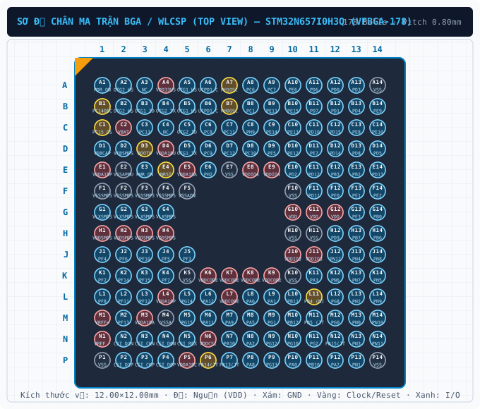
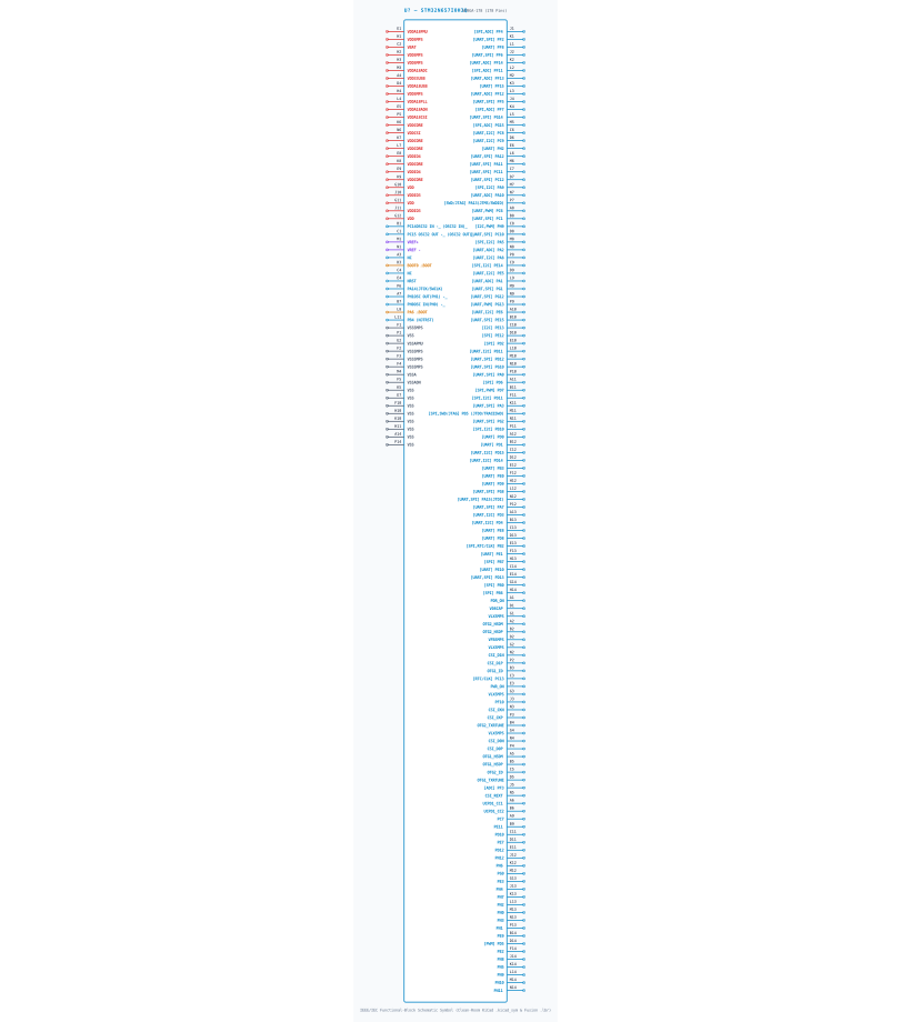
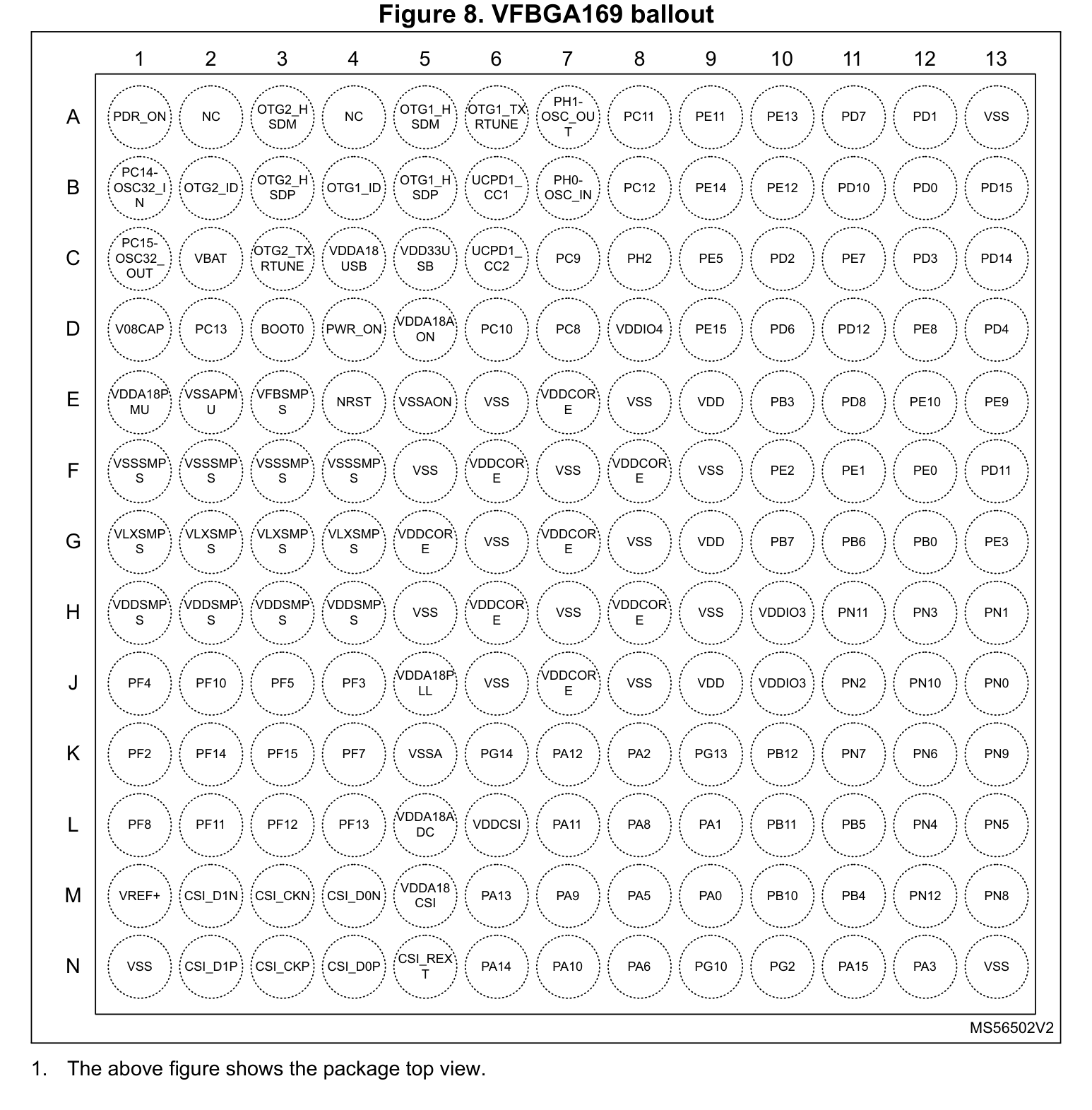
VFBGA-169(6x6) · 169P
| Pin | Symbol | Typ | Funktionsbeschreibung (DE) |
|---|---|---|---|
| A1 | PDR_ON | I/O | Multiplex-I/O- & Peripherie-Pin PDR_ON (General) |
| A2 | OTG2_HSDM | I/O | Multiplex-I/O- & Peripherie-Pin OTG2_HSDM (General) |
| A3 | NC | I/O | Multiplex-I/O- & Peripherie-Pin NC (General) |
| A4 | VDD33USB | Power | Versorgungsspannungseingang (VDD33USB — 3.3V VDD (Max 4.0V)) |
| A5 | OTG1_HSDM | I/O | Multiplex-I/O- & Peripherie-Pin OTG1_HSDM (General) |
| A6 | UCPD1_CC1 | I/O | Multiplex-I/O- & Peripherie-Pin UCPD1_CC1 (General) |
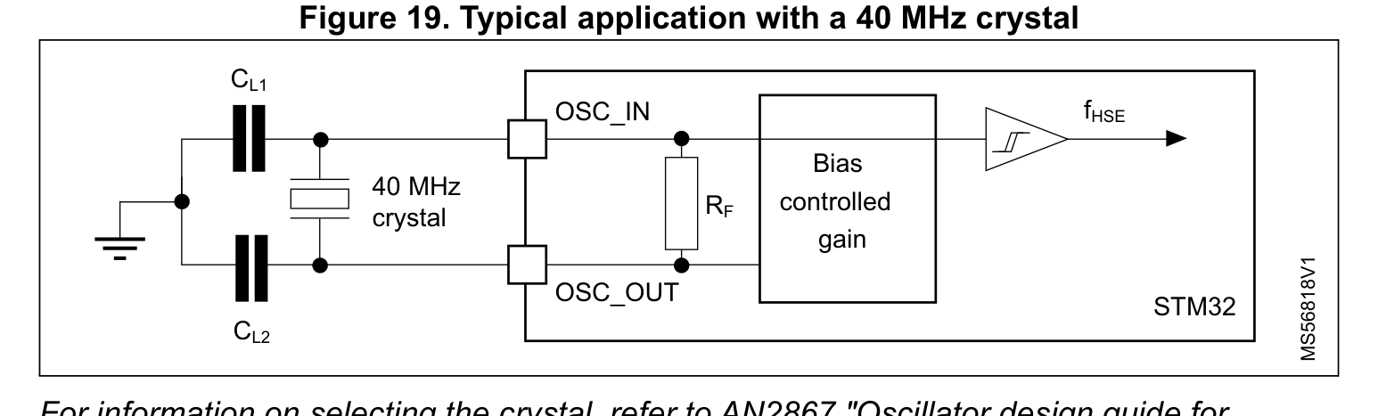
| A7 | PH1OSC OUT(PH1) -_ | I/O | Multiplex-I/O- & Peripherie-Pin PH1OSC OUT(PH1) -_ (RTC/CLK) |
| A8 | PC6 | I/O | Multiplex-I/O- & Peripherie-Pin PC6 (UART, PWM) |
| A9 | PC7 | I/O | Multiplex-I/O- & Peripherie-Pin PC7 (General) |
| A10 | PE6 | I/O | Multiplex-I/O- & Peripherie-Pin PE6 (UART, I2C, PWM) |
| A11 | PD6 | I/O | Multiplex-I/O- & Peripherie-Pin PD6 (SPI) |
| A12 | PD0 | I/O | Multiplex-I/O- & Peripherie-Pin PD0 (UART) |
| A13 | PD3 | I/O | Multiplex-I/O- & Peripherie-Pin PD3 (UART, I2C) |
| A14 | VSS | GND | Masseanschluss (VSS) |
| B1 | IOB1 | I/O | General Purpose Digital I/O Pin IOB1 |
| B2 | OTG2_HSDP | I/O | Multiplex-I/O- & Peripherie-Pin OTG2_HSDP (General) |
| B3 | OTG1_ID | I/O | Multiplex-I/O- & Peripherie-Pin OTG1_ID (General) |
| B4 | OTG2_TXRTUNE | I/O | Multiplex-I/O- & Peripherie-Pin OTG2_TXRTUNE (General) |
| B5 | OTG1_HSDP | I/O | Multiplex-I/O- & Peripherie-Pin OTG1_HSDP (General) |
| B6 | UCPD1_CC2 | I/O | Multiplex-I/O- & Peripherie-Pin UCPD1_CC2 (General) |
| B7 | PH0OSC IN(PH0) -_ | I/O | Multiplex-I/O- & Peripherie-Pin PH0OSC IN(PH0) -_ (RTC/CLK) |
| B8 | PC1 | I/O | Multiplex-I/O- & Peripherie-Pin PC1 (UART, SPI, PWM) |
| B9 | PE11 | I/O | Multiplex-I/O- & Peripherie-Pin PE11 (General) |
| B10 | PE15 | I/O | Multiplex-I/O- & Peripherie-Pin PE15 (UART, SPI) |
| B11 | PD7 | I/O | Multiplex-I/O- & Peripherie-Pin PD7 (SPI, PWM) |
| B12 | PD1 | I/O | Multiplex-I/O- & Peripherie-Pin PD1 (UART) |
| B13 | PD4 | I/O | Multiplex-I/O- & Peripherie-Pin PD4 (UART, I2C) |
| B14 | PE9 | I/O | Multiplex-I/O- & Peripherie-Pin PE9 (General) |
| C1 | IOC1 | I/O | General Purpose Digital I/O Pin IOC1 |
| C2 | VBAT | Power | Versorgungsspannungseingang (VBAT — 3.3V VDD (Max 4.0V)) |
| C3 | PC13 | I/O | Multiplex-I/O- & Peripherie-Pin PC13 (RTC/CLK) |
| C4 | NC | I/O | Multiplex-I/O- & Peripherie-Pin NC (General) |
| C5 | OTG2_ID | I/O | Multiplex-I/O- & Peripherie-Pin OTG2_ID (General) |
| C6 | PC8 | I/O | Multiplex-I/O- & Peripherie-Pin PC8 (UART, I2C) |
| C7 | PC11 | I/O | Multiplex-I/O- & Peripherie-Pin PC11 (UART, SPI, I2C) |
| C8 | PH9 | I/O | Multiplex-I/O- & Peripherie-Pin PH9 (I2C, PWM) |
| C9 | PE14 | I/O | Multiplex-I/O- & Peripherie-Pin PE14 (SPI, I2C) |
| C10 | PE13 | I/O | Multiplex-I/O- & Peripherie-Pin PE13 (I2C) |
| C11 | PD10 | I/O | Multiplex-I/O- & Peripherie-Pin PD10 (General) |
| C12 | PD15 | I/O | Multiplex-I/O- & Peripherie-Pin PD15 (UART, I2C) |
| C13 | PE8 | I/O | Multiplex-I/O- & Peripherie-Pin PE8 (UART) |
| C14 | PE10 | I/O | Multiplex-I/O- & Peripherie-Pin PE10 (UART) |
| D1 | V08CAP | I/O | Multiplex-I/O- & Peripherie-Pin V08CAP (General) |
| D2 | VFBSMPS | I/O | Multiplex-I/O- & Peripherie-Pin VFBSMPS (General) |
| D3 | BOOT0 | I | Reiner Eingangs-Pin BOOT0 (General) |
| D4 | VDDA18USB | Power | Versorgungsspannungseingang (VDDA18USB — 3.3V VDD (Max 4.0V)) |
| D5 | OTG1_TXRTUNE | I/O | Multiplex-I/O- & Peripherie-Pin OTG1_TXRTUNE (General) |
| D6 | PC9 | I/O | Multiplex-I/O- & Peripherie-Pin PC9 (UART, I2C, RTC/CLK) |
| D7 | PC12 | I/O | Multiplex-I/O- & Peripherie-Pin PC12 (UART, SPI) |
| D8 | PC10 | I/O | Multiplex-I/O- & Peripherie-Pin PC10 (UART, SPI, I2C) |
| D9 | PE5 | I/O | Multiplex-I/O- & Peripherie-Pin PE5 (UART, I2C, PWM) |
| D10 | PE12 | I/O | Multiplex-I/O- & Peripherie-Pin PE12 (SPI) |
| D11 | PE7 | I/O | Multiplex-I/O- & Peripherie-Pin PE7 (General) |
| D12 | PD14 | I/O | Multiplex-I/O- & Peripherie-Pin PD14 (UART, I2C) |
| D13 | PD8 | I/O | Multiplex-I/O- & Peripherie-Pin PD8 (UART) |
| D14 | PD5 | I/O | Multiplex-I/O- & Peripherie-Pin PD5 (PWM) |
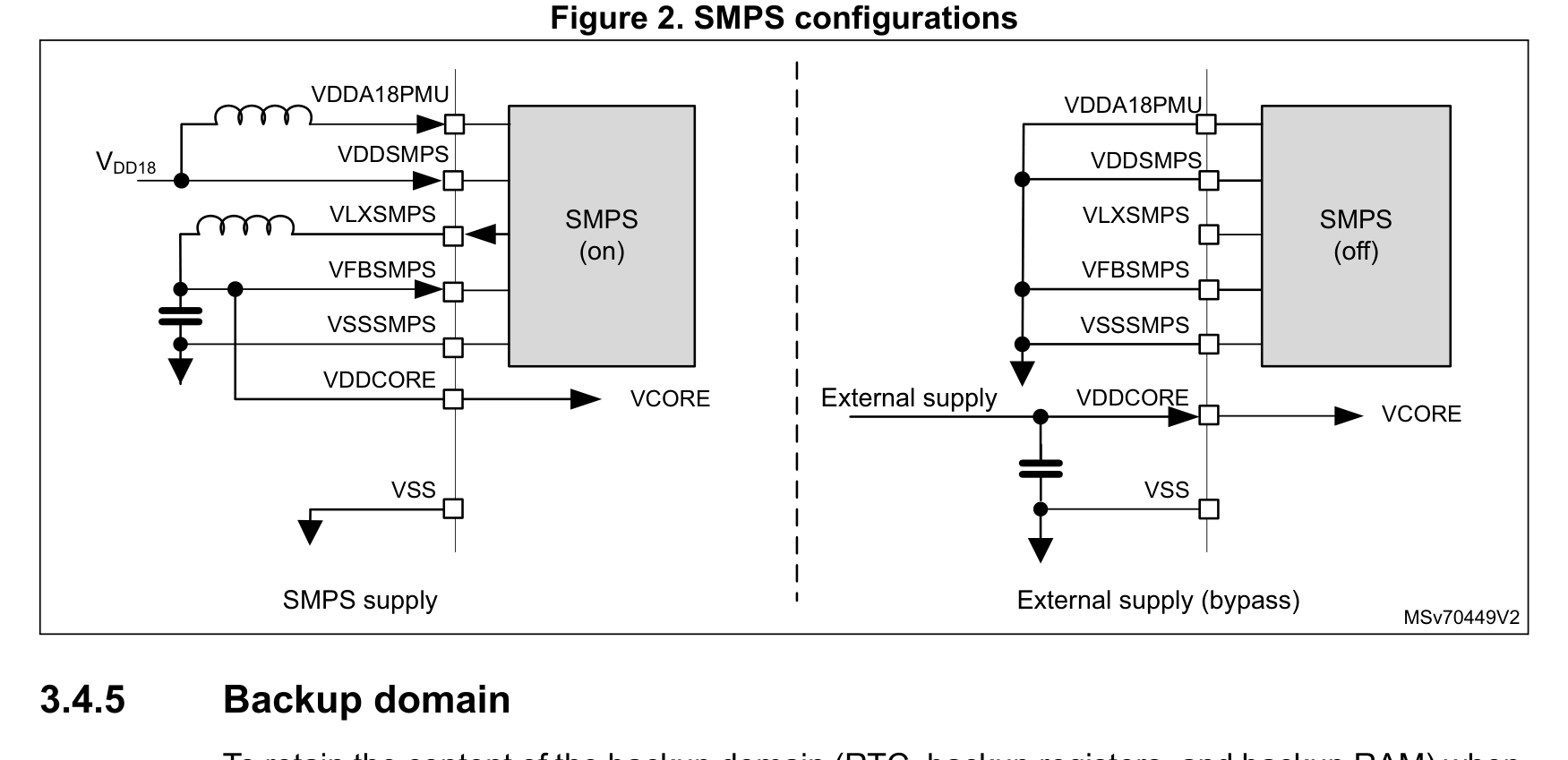
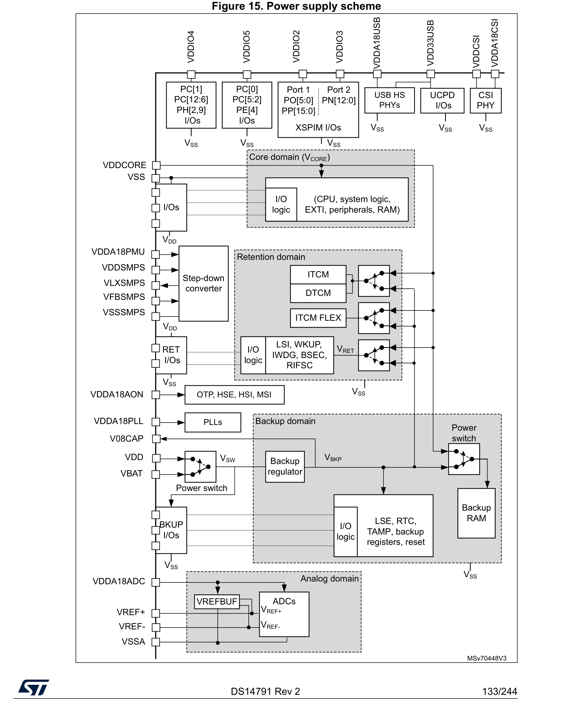
| E1 | VDDA18PMU | Power | Versorgungsspannungseingang (VDDA18PMU — 3.3V VDD (Max 4.0V)) |
| E2 | VSSAPMU | GND | Masseanschluss (VSSAPMU) |
| E3 | PWR_ON | I/O | Multiplex-I/O- & Peripherie-Pin PWR_ON (General) |
| E4 | NRST | I | Systemfreigabe & Hardware-Reset (NRST) |
| E5 | VDDA18AON | Power | Versorgungsspannungseingang (VDDA18AON — 3.3V VDD (Max 4.0V)) |
| E6 | PH2 | I/O | Multiplex-I/O- & Peripherie-Pin PH2 (UART) |
| E7 | VSS | GND | Masseanschluss (VSS) |
| E8 | VDDIO4 | Power | Versorgungsspannungseingang (VDDIO4 — 3.3V VDD (Max 4.0V)) |
| E9 | VDDIO4 | Power | Versorgungsspannungseingang (VDDIO4 — 3.3V VDD (Max 4.0V)) |
| E10 | PD2 | I/O | Multiplex-I/O- & Peripherie-Pin PD2 (SPI) |
| E11 | PD12 | I/O | Multiplex-I/O- & Peripherie-Pin PD12 (General) |
| E12 | PB3 | I/O | Multiplex-I/O- & Peripherie-Pin PB3 (UART) |
| E13 | PB2 | I/O | Multiplex-I/O- & Peripherie-Pin PB2 (SPI, RTC/CLK) |
| E14 | PD13 | I/O | Multiplex-I/O- & Peripherie-Pin PD13 (UART, SPI, PWM) |
| F1 | VSSSMPS | GND | Masseanschluss (VSSSMPS) |
| F2 | VSSSMPS | GND | Masseanschluss (VSSSMPS) |
| F3 | VSSSMPS | GND | Masseanschluss (VSSSMPS) |
| F4 | VSSSMPS | GND | Masseanschluss (VSSSMPS) |
| F5 | VSSAON | GND | Masseanschluss (VSSAON) |
| F10 | VSS | GND | Masseanschluss (VSS) |
| F11 | PD11 | I/O | Multiplex-I/O- & Peripherie-Pin PD11 (SPI, I2C) |
| F12 | PE0 | I/O | Multiplex-I/O- & Peripherie-Pin PE0 (UART) |
| F13 | PE1 | I/O | Multiplex-I/O- & Peripherie-Pin PE1 (UART) |
| F14 | PE2 | I/O | Multiplex-I/O- & Peripherie-Pin PE2 (General) |
| G1 | VLXSMPS | I/O | Multiplex-I/O- & Peripherie-Pin VLXSMPS (General) |
| G2 | VLXSMPS | I/O | Multiplex-I/O- & Peripherie-Pin VLXSMPS (General) |
| G3 | VLXSMPS | I/O | Multiplex-I/O- & Peripherie-Pin VLXSMPS (General) |
| G4 | VLXSMPS | I/O | Multiplex-I/O- & Peripherie-Pin VLXSMPS (General) |
| G10 | VDD | Power | Versorgungsspannungseingang (VDD — 3.3V VDD (Max 4.0V)) |
| G11 | VDD | Power | Versorgungsspannungseingang (VDD — 3.3V VDD (Max 4.0V)) |
| G12 | VDD | Power | Versorgungsspannungseingang (VDD — 3.3V VDD (Max 4.0V)) |
| G13 | PE3 | I/O | Multiplex-I/O- & Peripherie-Pin PE3 (General) |
| G14 | PB0 | I/O | Multiplex-I/O- & Peripherie-Pin PB0 (SPI) |
| H1 | VDDSMPS | Power | Versorgungsspannungseingang (VDDSMPS — 3.3V VDD (Max 4.0V)) |
| H2 | VDDSMPS | Power | Versorgungsspannungseingang (VDDSMPS — 3.3V VDD (Max 4.0V)) |
| H3 | VDDSMPS | Power | Versorgungsspannungseingang (VDDSMPS — 3.3V VDD (Max 4.0V)) |
| H4 | VDDSMPS | Power | Versorgungsspannungseingang (VDDSMPS — 3.3V VDD (Max 4.0V)) |
| H10 | VSS | GND | Masseanschluss (VSS) |
| H11 | VSS | GND | Masseanschluss (VSS) |
| H12 | PD9 | I/O | Multiplex-I/O- & Peripherie-Pin PD9 (UART) |
| H13 | PB7 | I/O | Multiplex-I/O- & Peripherie-Pin PB7 (SPI) |
| H14 | PB6 | I/O | Multiplex-I/O- & Peripherie-Pin PB6 (SPI) |
| J1 | PF4 | I/O | Multiplex-I/O- & Peripherie-Pin PF4 (SPI, ADC) |
| J2 | PF6 | I/O | Multiplex-I/O- & Peripherie-Pin PF6 (UART, SPI, ADC, PWM) |
| J3 | PF10 | I/O | Multiplex-I/O- & Peripherie-Pin PF10 (General) |
| J4 | PF5 | I/O | Multiplex-I/O- & Peripherie-Pin PF5 (UART, SPI) |
| J5 | PF3 | I/O | Multiplex-I/O- & Peripherie-Pin PF3 (ADC) |
| J10 | VDDIO3 | Power | Versorgungsspannungseingang (VDDIO3 — 3.3V VDD (Max 4.0V)) |
| J11 | VDDIO3 | Power | Versorgungsspannungseingang (VDDIO3 — 3.3V VDD (Max 4.0V)) |
| J12 | PN12 | I/O | Multiplex-I/O- & Peripherie-Pin PN12 (General) |
| J13 | PN4 | I/O | Multiplex-I/O- & Peripherie-Pin PN4 (General) |
| J14 | PN8 | I/O | Multiplex-I/O- & Peripherie-Pin PN8 (General) |
| K1 | PF2 | I/O | Multiplex-I/O- & Peripherie-Pin PF2 (UART, SPI) |
| K2 | PF14 | I/O | Multiplex-I/O- & Peripherie-Pin PF14 (UART, ADC) |
| K3 | PF15 | I/O | Multiplex-I/O- & Peripherie-Pin PF15 (UART) |
| K4 | PF7 | I/O | Multiplex-I/O- & Peripherie-Pin PF7 (SPI, ADC, PWM) |
| K5 | VSS | GND | Masseanschluss (VSS) |
| K6 | VDDCORE | Power | Versorgungsspannungseingang (VDDCORE — 3.3V VDD (Max 4.0V)) |
| K7 | VDDCORE | Power | Versorgungsspannungseingang (VDDCORE — 3.3V VDD (Max 4.0V)) |
| K8 | VDDCORE | Power | Versorgungsspannungseingang (VDDCORE — 3.3V VDD (Max 4.0V)) |
| K9 | VDDCORE | Power | Versorgungsspannungseingang (VDDCORE — 3.3V VDD (Max 4.0V)) |
| K10 | VSS | GND | Masseanschluss (VSS) |
| K11 | PA3 | I/O | Multiplex-I/O- & Peripherie-Pin PA3 (UART, SPI) |
| K12 | PN6 | I/O | Multiplex-I/O- & Peripherie-Pin PN6 (General) |
| K13 | PN7 | I/O | Multiplex-I/O- & Peripherie-Pin PN7 (General) |
| K14 | PN5 | I/O | Multiplex-I/O- & Peripherie-Pin PN5 (General) |
| L1 | PF8 | I/O | Multiplex-I/O- & Peripherie-Pin PF8 (UART) |
| L2 | PF11 | I/O | Multiplex-I/O- & Peripherie-Pin PF11 (SPI, ADC) |
| L3 | PF12 | I/O | Multiplex-I/O- & Peripherie-Pin PF12 (UART, ADC) |
| L4 | VDDA18PLL | Power | Versorgungsspannungseingang (VDDA18PLL — 3.3V VDD (Max 4.0V)) |
| L5 | PG14 | I/O | Multiplex-I/O- & Peripherie-Pin PG14 (UART, SPI) |
| L6 | PA12 | I/O | Multiplex-I/O- & Peripherie-Pin PA12 (UART, SPI, ADC) |
| L7 | VDDCORE | Power | Versorgungsspannungseingang (VDDCORE — 3.3V VDD (Max 4.0V)) |
| L8 | PA6 | I/O | Multiplex-I/O- & Peripherie-Pin PA6 (SPI, I2C, ADC) |
| L9 | PA1 | I/O | Multiplex-I/O- & Peripherie-Pin PA1 (UART, ADC, PWM) |
| L10 | PB11 | I/O | Multiplex-I/O- & Peripherie-Pin PB11 (UART, I2C, ADC) |
| L11 | PB4 (NJTRST) | I/O | Multiplex-I/O- & Peripherie-Pin PB4 (NJTRST) (UART, SPI, SWD/JTAG) |
| L12 | PG8 | I/O | Multiplex-I/O- & Peripherie-Pin PG8 (UART, SPI, PWM, RTC/CLK) |
| L13 | PN2 | I/O | Multiplex-I/O- & Peripherie-Pin PN2 (General) |
| L14 | PN9 | I/O | Multiplex-I/O- & Peripherie-Pin PN9 (General) |
| M1 | VREF+ | Analog | Multiplex-I/O- & Peripherie-Pin VREF+ (General) |
| M2 | PF13 | I/O | Multiplex-I/O- & Peripherie-Pin PF13 (UART, ADC) |
| M3 | VDDA18ADC | Power | Versorgungsspannungseingang (VDDA18ADC — 3.3V VDD (Max 4.0V)) |
| M4 | VSSA | GND | Masseanschluss (VSSA) |
| M5 | PG15 | I/O | Multiplex-I/O- & Peripherie-Pin PG15 (SPI, ADC) |
| M6 | PA11 | I/O | Multiplex-I/O- & Peripherie-Pin PA11 (UART, SPI, ADC) |
| M7 | PA9 | I/O | Multiplex-I/O- & Peripherie-Pin PA9 (SPI, I2C, ADC) |
| M8 | PA5 | I/O | Multiplex-I/O- & Peripherie-Pin PA5 (SPI, I2C, ADC, PWM) |
| M9 | PG1 | I/O | Multiplex-I/O- & Peripherie-Pin PG1 (UART, SPI) |
| M10 | PB12 | I/O | Multiplex-I/O- & Peripherie-Pin PB12 (UART, SPI) |
| M11 | PB5 (JTDO/TRACESWO) | I/O | Multiplex-I/O- & Peripherie-Pin PB5 (JTDO/TRACESWO) (SPI, SWD/JTAG) |
| M12 | PG0 | I/O | Multiplex-I/O- & Peripherie-Pin PG0 (General) |
| M13 | PN0 | I/O | Multiplex-I/O- & Peripherie-Pin PN0 (General) |
| M14 | PN10 | I/O | Multiplex-I/O- & Peripherie-Pin PN10 (General) |
| N1 | VREF - | Analog | Multiplex-I/O- & Peripherie-Pin VREF - (General) |
| N2 | CSI_D1N | I/O | Multiplex-I/O- & Peripherie-Pin CSI_D1N (General) |
| N3 | CSI_CKN | I/O | Multiplex-I/O- & Peripherie-Pin CSI_CKN (General) |
| N4 | CSI_D0N | I/O | Multiplex-I/O- & Peripherie-Pin CSI_D0N (General) |
| N5 | CSI_REXT | I/O | Multiplex-I/O- & Peripherie-Pin CSI_REXT (General) |
| N6 | VDDCSI | Power | Versorgungsspannungseingang (VDDCSI — 3.3V VDD (Max 4.0V)) |
| N7 | PA10 | I/O | Multiplex-I/O- & Peripherie-Pin PA10 (UART, ADC, PWM) |
| N8 | PA2 | I/O | Multiplex-I/O- & Peripherie-Pin PA2 (UART, ADC, PWM) |
| N9 | PG12 | I/O | Multiplex-I/O- & Peripherie-Pin PG12 (UART, SPI) |
| N10 | PG10 | I/O | Multiplex-I/O- & Peripherie-Pin PG10 (UART, SPI) |
| N11 | PG2 | I/O | Multiplex-I/O- & Peripherie-Pin PG2 (UART, SPI) |
| N12 | PA15(JTDI) | I/O | Multiplex-I/O- & Peripherie-Pin PA15(JTDI) (UART, SPI, SWD/JTAG) |
| N13 | PN3 | I/O | Multiplex-I/O- & Peripherie-Pin PN3 (General) |
| N14 | PN11 | I/O | Multiplex-I/O- & Peripherie-Pin PN11 (General) |
| P1 | VSS | GND | Masseanschluss (VSS) |
| P2 | CSI_D1P | I/O | Multiplex-I/O- & Peripherie-Pin CSI_D1P (General) |
| P3 | CSI_CKP | I/O | Multiplex-I/O- & Peripherie-Pin CSI_CKP (General) |
| P4 | CSI_D0P | I/O | Multiplex-I/O- & Peripherie-Pin CSI_D0P (General) |
| P5 | VDDA18CSI | Power | Versorgungsspannungseingang (VDDA18CSI — 3.3V VDD (Max 4.0V)) |
| P6 | PA14(JTCK/SWCLK) | I/O | Multiplex-I/O- & Peripherie-Pin PA14(JTCK/SWCLK) (SWD/JTAG) |
| P7 | PA13(JTMS/SWDIO) | I/O | Multiplex-I/O- & Peripherie-Pin PA13(JTMS/SWDIO) (SWD/JTAG) |
| P8 | PA8 | I/O | Multiplex-I/O- & Peripherie-Pin PA8 (UART, I2C, ADC, RTC/CLK) |
| P9 | PG13 | I/O | Multiplex-I/O- & Peripherie-Pin PG13 (UART, PWM) |
| P10 | PA0 | I/O | Multiplex-I/O- & Peripherie-Pin PA0 (UART, SPI, ADC, PWM) |
| P11 | PB10 | I/O | Multiplex-I/O- & Peripherie-Pin PB10 (SPI, I2C, ADC) |
| P12 | PA7 | I/O | Multiplex-I/O- & Peripherie-Pin PA7 (UART, SPI, ADC) |
| P13 | PN1 | I/O | Multiplex-I/O- & Peripherie-Pin PN1 (General) |
| P14 | VSS | GND | Masseanschluss (VSS) |
| Bauteilbezeichner / Ersatz-MPN | Wert / Gehäuse | Funktion & PCB-Layout-Regel |
|---|---|---|
| N/A BOM | Per application circuit VFBGA-178 | Leiterbahnbreiten für Nennstrom dimensionieren und IPC-2221 Isolationsabstände einhalten. |
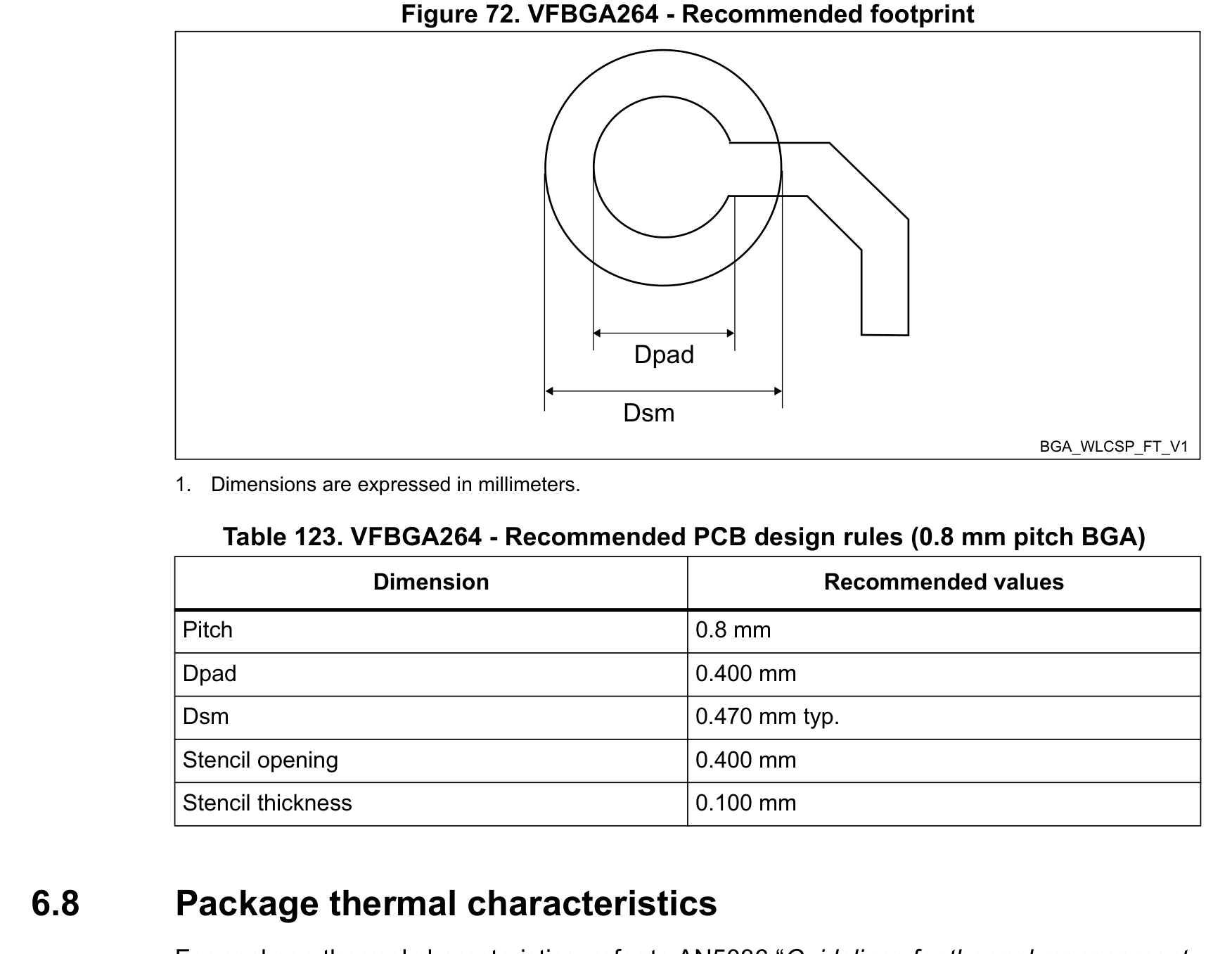
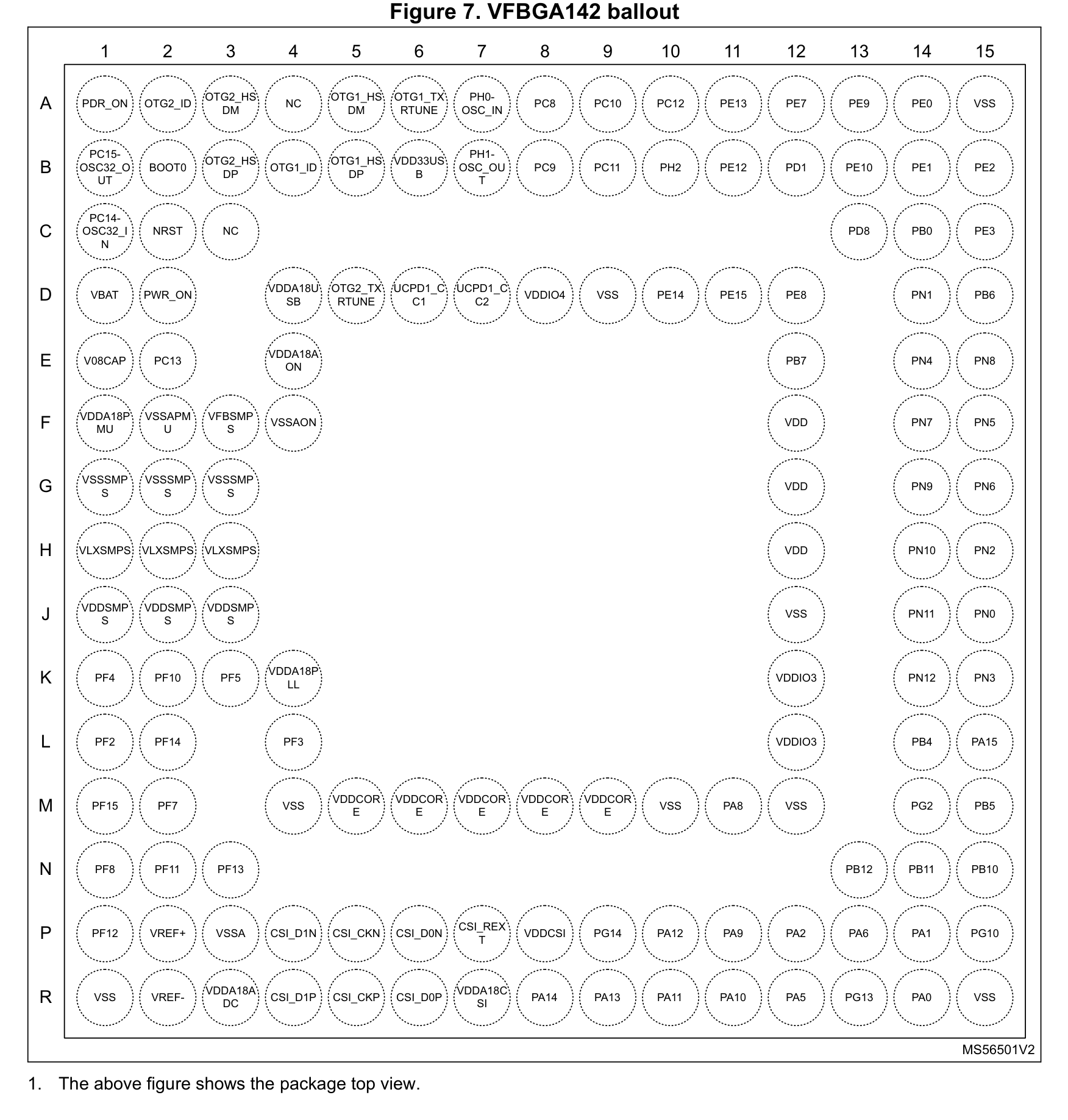
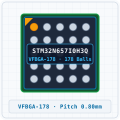
Das Bauteil STM32N657I0H3Q von ST im VFBGA-178-Gehäuse besitzt 178 Pins mit einem Rastermaß (Pitch) von 0.80 mm. Wichtige Pins: A1 (PDR_ON: Multiplex-I/O- & Peripherie-Pin PDR_ON (General)), A2 (OTG2_HSDM: Multiplex-I/O- & Peripherie-Pin OTG2_HSDM (General)), A3 (NC: Multiplex-I/O- & Peripherie-Pin NC (General)), A4 (VDD33USB: Versorgungsspannungseingang (VDD33USB — 3.3V VDD (Max 4.0V))), A5 (OTG1_HSDM: Multiplex-I/O- & Peripherie-Pin OTG1_HSDM (General)), A6 (UCPD1_CC1: Multiplex-I/O- & Peripherie-Pin UCPD1_CC1 (General)).
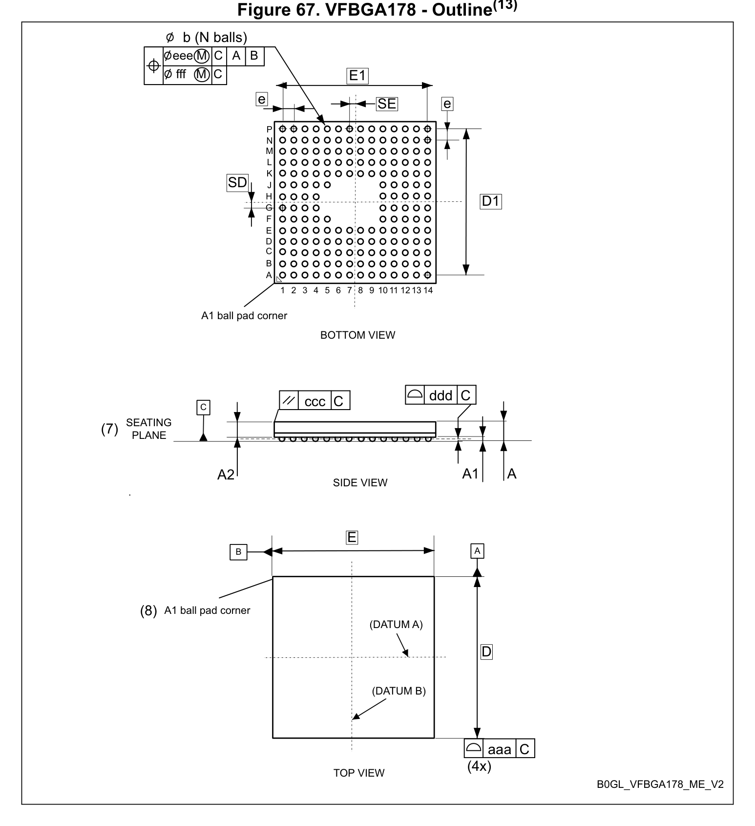
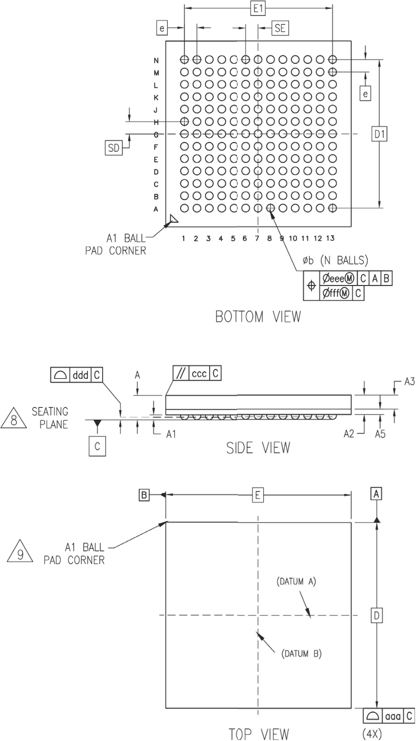
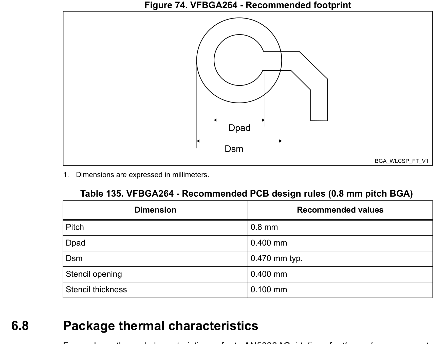
Gemäß Datenblatt und IPC-7351B (Density Level B Nominal) betragen die Gehäusemaße des STM32N657I0H3Q (VFBGA-178) 12.00 × 12.00 mm bei einem Pitch e = 0.80 mm und 178 Kupfer-Pads.
Auf dieser Seite können Sie das vollständig verifizierte CAD-Bibliothekspaket für STM32N657I0H3Q (ST, VFBGA-178) unter der Open-Hardware-Lizenz CERN-OHL-P-2.0 kostenlos herunterladen: KiCad 8 Footprint (.kicad_mod), Schaltplansymbol (.kicad_sym), Fusion 360 / Eagle (.lbr) und 3D STEP AP214 / WebGL GLB.
| Pin-Nr. | Signalname | Elektrischer Typ | Funktionsbeschreibung & Schaltungshinweise |
|---|---|---|---|
| A1 | PDR_ON | Digital_IO | Signalanschluss PDR_ON (Richtung: I/O, Spannungsbereich: 3.3V VDD (Max 4.0V)). Alternative Multiplex-Funktionen: PDR_ON. Unterstützte Bus-Schnittstellen: General. |
| A2 | OTG2_HSDM | Digital_IO | Signalanschluss OTG2_HSDM (Richtung: I/O, Spannungsbereich: 3.3V VDD (Max 4.0V)). Alternative Multiplex-Funktionen: OTG2_HSDM. Unterstützte Bus-Schnittstellen: General. |
| A3 | NC | NC | Signalanschluss NC (Richtung: I/O, Spannungsbereich: 3.3V VDD (Max 4.0V)). Alternative Multiplex-Funktionen: NC. Unterstützte Bus-Schnittstellen: General. |
| A4 | VDD33USB | Power_In | Positiver Versorgungseingang (VDD33USB) im Spannungsbereich 3.3V VDD (Max 4.0V) (Max. 4.0V). |
| A5 | OTG1_HSDM | Digital_IO | Signalanschluss OTG1_HSDM (Richtung: I/O, Spannungsbereich: 3.3V VDD (Max 4.0V)). Alternative Multiplex-Funktionen: OTG1_HSDM. Unterstützte Bus-Schnittstellen: General. |
| A6 | UCPD1_CC1 | Digital_IO | Signalanschluss UCPD1_CC1 (Richtung: I/O, Spannungsbereich: 3.3V VDD (Max 4.0V)). Alternative Multiplex-Funktionen: UCPD1_CC1. Unterstützte Bus-Schnittstellen: General. |
| A7 | PH1OSC OUT(PH1) -_ | Digital_IO | Signalanschluss PH1OSC OUT(PH1) -_ (Richtung: I/O, Spannungsbereich: 3.3V VDD (Max 4.0V)). Alternative Multiplex-Funktionen: PH1OSC OUT(PH1) -_. Unterstützte Bus-Schnittstellen: RTC/CLK. |
| A8 | PC6 | Digital_IO | Signalanschluss PC6 (Richtung: I/O, Spannungsbereich: 3.3V VDD (Max 4.0V)). Alternative Multiplex-Funktionen: PC6. Unterstützte Bus-Schnittstellen: UART, PWM. |
| A9 | PC7 | Digital_IO | Signalanschluss PC7 (Richtung: I/O, Spannungsbereich: 3.3V VDD (Max 4.0V)). Alternative Multiplex-Funktionen: PC7. Unterstützte Bus-Schnittstellen: General. |
| A10 | PE6 | Digital_IO | Signalanschluss PE6 (Richtung: I/O, Spannungsbereich: 3.3V VDD (Max 4.0V)). Alternative Multiplex-Funktionen: I2C1_SDA. Unterstützte Bus-Schnittstellen: UART, I2C, PWM. |
| A11 | PD6 | Digital_IO | Signalanschluss PD6 (Richtung: I/O, Spannungsbereich: 3.3V VDD (Max 4.0V)). Alternative Multiplex-Funktionen: SPI2_MISO. Unterstützte Bus-Schnittstellen: SPI. |
| A12 | PD0 | Digital_IO | Signalanschluss PD0 (Richtung: I/O, Spannungsbereich: 3.3V VDD (Max 4.0V)). Alternative Multiplex-Funktionen: PD0. Unterstützte Bus-Schnittstellen: UART. |
| A13 | PD3 | Digital_IO | Signalanschluss PD3 (Richtung: I/O, Spannungsbereich: 3.3V VDD (Max 4.0V)). Alternative Multiplex-Funktionen: I2C2_SMBA. Unterstützte Bus-Schnittstellen: UART, I2C. |
| A14 | VSS | GND | Elektrischer 0V-Masserückführungsanschluss (VSS) für Kernlogik, I/O-Treiber und Analogblöcke. |
| B1 | IOB1 | Digital_IO | General Purpose Digital I/O Pin IOB1 |
| B2 | OTG2_HSDP | Digital_IO | Signalanschluss OTG2_HSDP (Richtung: I/O, Spannungsbereich: 3.3V VDD (Max 4.0V)). Alternative Multiplex-Funktionen: OTG2_HSDP. Unterstützte Bus-Schnittstellen: General. |
| B3 | OTG1_ID | Digital_IO | Signalanschluss OTG1_ID (Richtung: I/O, Spannungsbereich: 3.3V VDD (Max 4.0V)). Alternative Multiplex-Funktionen: OTG1_ID. Unterstützte Bus-Schnittstellen: General. |
| B4 | OTG2_TXRTUNE | Digital_IO | Signalanschluss OTG2_TXRTUNE (Richtung: I/O, Spannungsbereich: 3.3V VDD (Max 4.0V)). Alternative Multiplex-Funktionen: OTG2_TXRTUNE. Unterstützte Bus-Schnittstellen: General. |
| B5 | OTG1_HSDP | Digital_IO | Signalanschluss OTG1_HSDP (Richtung: I/O, Spannungsbereich: 3.3V VDD (Max 4.0V)). Alternative Multiplex-Funktionen: OTG1_HSDP. Unterstützte Bus-Schnittstellen: General. |
| B6 | UCPD1_CC2 | Digital_IO | Signalanschluss UCPD1_CC2 (Richtung: I/O, Spannungsbereich: 3.3V VDD (Max 4.0V)). Alternative Multiplex-Funktionen: UCPD1_CC2. Unterstützte Bus-Schnittstellen: General. |
| B7 | PH0OSC IN(PH0) -_ | Digital_IO | Signalanschluss PH0OSC IN(PH0) -_ (Richtung: I/O, Spannungsbereich: 3.3V VDD (Max 4.0V)). Alternative Multiplex-Funktionen: PH0OSC IN(PH0) -_. Unterstützte Bus-Schnittstellen: RTC/CLK. |
| B8 | PC1 | Digital_IO | Signalanschluss PC1 (Richtung: I/O, Spannungsbereich: 3.3V VDD (Max 4.0V)). Alternative Multiplex-Funktionen: SPI2_NSS. Unterstützte Bus-Schnittstellen: UART, SPI, PWM. |
| B9 | PE11 | Digital_IO | Signalanschluss PE11 (Richtung: I/O, Spannungsbereich: 3.3V VDD (Max 4.0V)). Alternative Multiplex-Funktionen: PE11. Unterstützte Bus-Schnittstellen: General. |
| B10 | PE15 | Digital_IO | Signalanschluss PE15 (Richtung: I/O, Spannungsbereich: 3.3V VDD (Max 4.0V)). Alternative Multiplex-Funktionen: SPI5_SCK. Unterstützte Bus-Schnittstellen: UART, SPI. |
| B11 | PD7 | Digital_IO | Signalanschluss PD7 (Richtung: I/O, Spannungsbereich: 3.3V VDD (Max 4.0V)). Alternative Multiplex-Funktionen: SPI2_MOSI, SPI3_NSS. Unterstützte Bus-Schnittstellen: SPI, PWM. |
| B12 | PD1 | Digital_IO | Signalanschluss PD1 (Richtung: I/O, Spannungsbereich: 3.3V VDD (Max 4.0V)). Alternative Multiplex-Funktionen: PD1. Unterstützte Bus-Schnittstellen: UART. |
| B13 | PD4 | Digital_IO | Signalanschluss PD4 (Richtung: I/O, Spannungsbereich: 3.3V VDD (Max 4.0V)). Alternative Multiplex-Funktionen: PD4. Unterstützte Bus-Schnittstellen: UART, I2C. |
| B14 | PE9 | Digital_IO | Signalanschluss PE9 (Richtung: I/O, Spannungsbereich: 3.3V VDD (Max 4.0V)). Alternative Multiplex-Funktionen: PE9. Unterstützte Bus-Schnittstellen: General. |
| C1 | IOC1 | Digital_IO | General Purpose Digital I/O Pin IOC1 |
| C2 | VBAT | Power_In | Positiver Versorgungseingang (VBAT) im Spannungsbereich 3.3V VDD (Max 4.0V) (Max. 4.0V). |
| C3 | PC13 | Digital_IO | Signalanschluss PC13 (Richtung: I/O, Spannungsbereich: 3.3V VDD (Max 4.0V)). Alternative Multiplex-Funktionen: PC13. Unterstützte Bus-Schnittstellen: RTC/CLK. |
| C4 | NC | NC | Signalanschluss NC (Richtung: I/O, Spannungsbereich: 3.3V VDD (Max 4.0V)). Alternative Multiplex-Funktionen: NC. Unterstützte Bus-Schnittstellen: General. |
| C5 | OTG2_ID | Digital_IO | Signalanschluss OTG2_ID (Richtung: I/O, Spannungsbereich: 3.3V VDD (Max 4.0V)). Alternative Multiplex-Funktionen: OTG2_ID. Unterstützte Bus-Schnittstellen: General. |
| C6 | PC8 | Digital_IO | Signalanschluss PC8 (Richtung: I/O, Spannungsbereich: 3.3V VDD (Max 4.0V)). Alternative Multiplex-Funktionen: I2C3_SMBA. Unterstützte Bus-Schnittstellen: UART, I2C. |
| C7 | PC11 | Digital_IO | Signalanschluss PC11 (Richtung: I/O, Spannungsbereich: 3.3V VDD (Max 4.0V)). Alternative Multiplex-Funktionen: I2C4_SDA, SPI3_MISO. Unterstützte Bus-Schnittstellen: UART, SPI, I2C. |
| C8 | PH9 | Digital_IO | Signalanschluss PH9 (Richtung: I/O, Spannungsbereich: 3.3V VDD (Max 4.0V)). Alternative Multiplex-Funktionen: I2C1_SCL. Unterstützte Bus-Schnittstellen: I2C, PWM. |
| C9 | PE14 | Digital_IO | Signalanschluss PE14 (Richtung: I/O, Spannungsbereich: 3.3V VDD (Max 4.0V)). Alternative Multiplex-Funktionen: I2C4_SDA, SPI4_MOSI_SAI2MCLKB. Unterstützte Bus-Schnittstellen: SPI, I2C. |
| C10 | PE13 | Digital_IO | Signalanschluss PE13 (Richtung: I/O, Spannungsbereich: 3.3V VDD (Max 4.0V)). Alternative Multiplex-Funktionen: PE13. Unterstützte Bus-Schnittstellen: I2C. |
| C11 | PD10 | Digital_IO | Signalanschluss PD10 (Richtung: I/O, Spannungsbereich: 3.3V VDD (Max 4.0V)). Alternative Multiplex-Funktionen: PD10. Unterstützte Bus-Schnittstellen: General. |
| C12 | PD15 | Digital_IO | Signalanschluss PD15 (Richtung: I/O, Spannungsbereich: 3.3V VDD (Max 4.0V)). Alternative Multiplex-Funktionen: I2C2_SDA. Unterstützte Bus-Schnittstellen: UART, I2C. |
| C13 | PE8 | Digital_IO | Signalanschluss PE8 (Richtung: I/O, Spannungsbereich: 3.3V VDD (Max 4.0V)). Alternative Multiplex-Funktionen: PE8. Unterstützte Bus-Schnittstellen: UART. |
| C14 | PE10 | Digital_IO | Signalanschluss PE10 (Richtung: I/O, Spannungsbereich: 3.3V VDD (Max 4.0V)). Alternative Multiplex-Funktionen: PE10. Unterstützte Bus-Schnittstellen: UART. |
| D1 | V08CAP | Digital_IO | Signalanschluss V08CAP (Richtung: I/O, Spannungsbereich: 3.3V VDD (Max 4.0V)). Alternative Multiplex-Funktionen: V08CAP. Unterstützte Bus-Schnittstellen: General. |
| D2 | VFBSMPS | Digital_IO | Signalanschluss VFBSMPS (Richtung: I/O, Spannungsbereich: 3.3V VDD (Max 4.0V)). Alternative Multiplex-Funktionen: VFBSMPS. Unterstützte Bus-Schnittstellen: General. |
| D3 | BOOT0 | Digital_IO | Signalanschluss BOOT0 (Richtung: I, Spannungsbereich: 3.3V VDD (Max 4.0V)). Alternative Multiplex-Funktionen: BOOT0. Unterstützte Bus-Schnittstellen: General. |
| D4 | VDDA18USB | Power_In | Positiver Versorgungseingang (VDDA18USB) im Spannungsbereich 3.3V VDD (Max 4.0V) (Max. 4.0V). |
| D5 | OTG1_TXRTUNE | Digital_IO | Signalanschluss OTG1_TXRTUNE (Richtung: I/O, Spannungsbereich: 3.3V VDD (Max 4.0V)). Alternative Multiplex-Funktionen: OTG1_TXRTUNE. Unterstützte Bus-Schnittstellen: General. |
| D6 | PC9 | Digital_IO | Signalanschluss PC9 (Richtung: I/O, Spannungsbereich: 3.3V VDD (Max 4.0V)). Alternative Multiplex-Funktionen: I2C3_SDA. Unterstützte Bus-Schnittstellen: UART, I2C, RTC/CLK. |
| D7 | PC12 | Digital_IO | Signalanschluss PC12 (Richtung: I/O, Spannungsbereich: 3.3V VDD (Max 4.0V)). Alternative Multiplex-Funktionen: SPI6_SCK, SPI3_MOSI. Unterstützte Bus-Schnittstellen: UART, SPI. |
| D8 | PC10 | Digital_IO | Signalanschluss PC10 (Richtung: I/O, Spannungsbereich: 3.3V VDD (Max 4.0V)). Alternative Multiplex-Funktionen: SPI3_SCK. Unterstützte Bus-Schnittstellen: UART, SPI, I2C. |
| D9 | PE5 | Digital_IO | Signalanschluss PE5 (Richtung: I/O, Spannungsbereich: 3.3V VDD (Max 4.0V)). Alternative Multiplex-Funktionen: I2C1_SCL. Unterstützte Bus-Schnittstellen: UART, I2C, PWM. |
| D10 | PE12 | Digital_IO | Signalanschluss PE12 (Richtung: I/O, Spannungsbereich: 3.3V VDD (Max 4.0V)). Alternative Multiplex-Funktionen: PE12. Unterstützte Bus-Schnittstellen: SPI. |
| D11 | PE7 | Digital_IO | Signalanschluss PE7 (Richtung: I/O, Spannungsbereich: 3.3V VDD (Max 4.0V)). Alternative Multiplex-Funktionen: PE7. Unterstützte Bus-Schnittstellen: General. |
| D12 | PD14 | Digital_IO | Signalanschluss PD14 (Richtung: I/O, Spannungsbereich: 3.3V VDD (Max 4.0V)). Alternative Multiplex-Funktionen: I2C2_SCL. Unterstützte Bus-Schnittstellen: UART, I2C. |
| D13 | PD8 | Digital_IO | Signalanschluss PD8 (Richtung: I/O, Spannungsbereich: 3.3V VDD (Max 4.0V)). Alternative Multiplex-Funktionen: PD8. Unterstützte Bus-Schnittstellen: UART. |
| D14 | PD5 | Digital_IO | Signalanschluss PD5 (Richtung: I/O, Spannungsbereich: 3.3V VDD (Max 4.0V)). Alternative Multiplex-Funktionen: PD5. Unterstützte Bus-Schnittstellen: PWM. |
| E1 | VDDA18PMU | Power_In | Positiver Versorgungseingang (VDDA18PMU) im Spannungsbereich 3.3V VDD (Max 4.0V) (Max. 4.0V). |
| E2 | VSSAPMU | GND | Elektrischer 0V-Masserückführungsanschluss (VSSAPMU) für Kernlogik, I/O-Treiber und Analogblöcke. |
| E3 | PWR_ON | Digital_IO | Signalanschluss PWR_ON (Richtung: I/O, Spannungsbereich: 3.3V VDD (Max 4.0V)). Alternative Multiplex-Funktionen: PWR_ON. Unterstützte Bus-Schnittstellen: General. |
| E4 | NRST | Digital_IO | Aktiv-niedriger Hardware-Reset-Anschluss (NRST): Low-Pegel setzt Prozessorkern und Peripherie zurück. |
| E5 | VDDA18AON | Power_In | Positiver Versorgungseingang (VDDA18AON) im Spannungsbereich 3.3V VDD (Max 4.0V) (Max. 4.0V). |
| E6 | PH2 | Digital_IO | Signalanschluss PH2 (Richtung: I/O, Spannungsbereich: 3.3V VDD (Max 4.0V)). Alternative Multiplex-Funktionen: PH2. Unterstützte Bus-Schnittstellen: UART. |
| E7 | VSS | GND | Elektrischer 0V-Masserückführungsanschluss (VSS) für Kernlogik, I/O-Treiber und Analogblöcke. |
| E8 | VDDIO4 | Power_In | Positiver Versorgungseingang (VDDIO4) im Spannungsbereich 3.3V VDD (Max 4.0V) (Max. 4.0V). |