STM32F427IGH6 (UFBGA-201) — Symbol, Footprint IPC-7351B & 3D STEP Model

STM32F427IGH6

STID: C1337379UFBGA-201 · 201 Pins · Pitch 0.65mmIPC-7351B Verified5.0 (0)
SYNCHRONISIERTER 4D-CROSS-PROBE-MODUSKlicken oder berühren Sie einen Pin, um ihn zeitgleich in Symbol, Footprint und 3D hervorzuheben
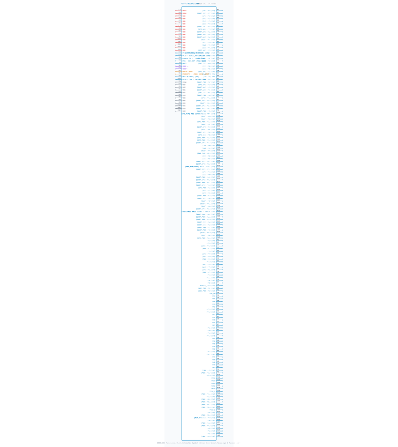
1. SCHALTPLANSYMBOL
U1 · STM32F427IGH6 (UFBGA-201)A1PE3A2PE2A3PE1A4PE0A5PB8A6PB5A7PG14A8PG13A9PB4 (NJTRST)A10PB3 (JTDO/TRA11PD7A12PC12A13PA15 (JTDI)A14PA14 (JTCK -A15PA13 (JTMS -B1PE4B2PE5B3PE6B4PB9B5PB7B6PB6B7PG15B8PG12B9PG11B10PG10B11PD6B12PD0B13PC11B14PC10B15PA12C1VBATC2PI7C3PI6C4PI5C5VDDC6PDR_ONC7VDDC8VDDC9VDDC10PG9C11PD5C12PD1C13PI3C14PI2C15PA11D1PC13D2PI8D3PI9D4PI4D5VSSD6BOOT0D7VSSD8VSSD9VSSD10PD4D11PD3D12PD2D13PH15D14PI1D15PA10E1PC14 - OSC32E2PF0E3PI10E4PI11E12PH13E13PH14E14PI0E15PA9F1IOF1F2VSSF3VDDF4PH2F6PF6F7PF7F8PF8F9PF9F10PF10F12VSSF13VCAP_2F14PC9F15PA8G1PH0OSC IN -_G2VSSG3VDDG4PH3G6PG6G7PG7G8PG8G9PG9G10PG10G12VSSG13VDDG14PC8G15PC7H1PH1 - OSC_OUH2PF2H3PF1H4PH4H6PH6H7PH7H8PH8R15PB15R14PB14R13PB11R12PB10R11PE15R10PE12R9PE10R8PE7R7PF14R6PF11R5PB0R4PB1R3PA7R2PA3R1VDDAP15PD8P14PD9P13PB13P12PB12P11PE14P10PE11P9PE9P8PE8P7PF15P6PF12P5PC5P4PA5P3PA6P2PA2P1VREF+N15PD10N14PD11N13PD12N12PH7N11PE13N10VDDN9VDDN8VDDN7PG0N6PF13N5PC4N4PA4N3PA0WKUP - (PN2PA1N1VREF –M15PD13M14PD14M13PH9M12PH8M11PH6M10VCAP_1M9VSSM8VSSM7PG1M6PB2BOOT1 - (M5PC3M4PC2M3PC1M2PC0M1VSSAL15PG2L14PD15L13PH10L12PH11L4BYPASS_ REGL3PF8L2PF9L1PF10K15PG3K14PG4K13PG5K12PH12K10PK10K9PK9K8PK8K7PK7K6PK6K4VDDK3PF5K2PF6K1PF7J15PG6J14PG7J13VDDJ12VDDJ10PJ10J9PJ9J8PJ8J7PJ7J6PJ6J4PH5J3PF4J2PF3J1NRSTH15PC6H14PG8H13VDDH12VSSH10PH10H9PH9Grid Pitch = 2.54mm (IEEE-315)-17.8-12.7-7.6-2.52.57.612.717.8134.6129.5124.5119.4114.3109.2104.199.194.088.983.878.773.768.663.558.453.348.343.238.133.027.922.917.812.77.62.5-2.5-7.6-12.7-17.8-22.9-27.9-33.0-38.1-43.2-48.3-53.3-58.4-63.5-68.6-73.7-78.7-83.8-88.9-94.0-99.1-104.1-109.2-114.3-119.4-124.5-129.5-134.6mm
2. 2D-FOOTPRINT
A1B1C1D1E1F1G1H1J1K1L1M1N1P1R1A2B2C2D2E2F2G2H2J2K2L2M2N2P2R2A3B3C3D3E3F3G3H3J3K3L3M3N3P3R3A4B4C4D4E4F4G4H4J4K4L4M4N4P4R4A5B5C5D5M5N5P5R5A6B6C6D6F6G6H6J6K6M6N6P6R6A7B7C7D7F7G7H7J7K7M7N7P7R7A8B8C8D8F8G8H8J8K8M8N8P8R8A9B9C9D9F9G9H9J9K9M9N9P9R9A10B10C10D10F10G10H10J10K10M10N10P10R10A11B11C11D11M11N11P11R11A12B12C12D12E12F12G12H12J12K12L12M12N12P12R12A13B13C13D13E13F13G13H13J13K13L13M13N13P13R13A14B14C14D14E14F14G14H14J14K14L14M14N14P14R14A15B15C15D15E15F15G15H15J15K15L15M15N15P15R15E=10.00mm · Pitch e=0.65mmD=10.00mm-7-5-3-113577531-1-3-5-7mm
3. 3D-MODELL
Gehäusekörper: 10.00mm × 10.00mm · Raster: 0.65mm · Linealschritt: 1.00mmSynchronisiert <100ms

Synchronisierte Pinbelegung (Symbol / 2D / 3D) (201/201)

Klicken oder berühren Sie einen Pin, um ihn zeitgleich in Symbol, Footprint und 3D hervorzuheben
PinSymbolTypFunktionsbeschreibung (DE)
A1PE3I/OMultiplex-I/O- & Peripherie-Pin PE3 (General)
A2PE2I/OMultiplex-I/O- & Peripherie-Pin PE2 (SPI)
A3PE1I/OMultiplex-I/O- & Peripherie-Pin PE1 (UART)
A4PE0I/OMultiplex-I/O- & Peripherie-Pin PE0 (UART)
A5PB8I/OMultiplex-I/O- & Peripherie-Pin PB8 (I2C, PWM)
A6PB5I/OMultiplex-I/O- & Peripherie-Pin PB5 (SPI, I2C, PWM, CAN)
A7PG14I/OMultiplex-I/O- & Peripherie-Pin PG14 (UART, SPI)
A8PG13I/OMultiplex-I/O- & Peripherie-Pin PG13 (UART, SPI)
A9PB4 (NJTRST)I/OMultiplex-I/O- & Peripherie-Pin PB4 (NJTRST) (SPI, SWD/JTAG)
A10PB3 (JTDO/TRACE SWO)I/OMultiplex-I/O- & Peripherie-Pin PB3 (JTDO/TRACE SWO) (SPI, PWM, SWD/JTAG)
A11PD7I/OMultiplex-I/O- & Peripherie-Pin PD7 (UART)
A12PC12I/OMultiplex-I/O- & Peripherie-Pin PC12 (UART, SPI)
A13PA15 (JTDI)I/OMultiplex-I/O- & Peripherie-Pin PA15 (JTDI) (SPI, SWD/JTAG)
A14PA14 (JTCK - SWCLK)I/OMultiplex-I/O- & Peripherie-Pin PA14 (JTCK - SWCLK) (SWD/JTAG)
A15PA13 (JTMS - SWDIO)I/OMultiplex-I/O- & Peripherie-Pin PA13 (JTMS - SWDIO) (SWD/JTAG)
B1PE4I/OMultiplex-I/O- & Peripherie-Pin PE4 (SPI)
B2PE5I/OMultiplex-I/O- & Peripherie-Pin PE5 (SPI)
B3PE6I/OMultiplex-I/O- & Peripherie-Pin PE6 (SPI)
B4PB9I/OMultiplex-I/O- & Peripherie-Pin PB9 (SPI, I2C, PWM, CAN)
B5PB7I/OMultiplex-I/O- & Peripherie-Pin PB7 (UART, PWM)
B6PB6I/OMultiplex-I/O- & Peripherie-Pin PB6 (UART, PWM, CAN)
B7PG15I/OMultiplex-I/O- & Peripherie-Pin PG15 (UART)
B8PG12I/OMultiplex-I/O- & Peripherie-Pin PG12 (UART, SPI)
B9PG11I/OMultiplex-I/O- & Peripherie-Pin PG11 (General)
B10PG10I/OMultiplex-I/O- & Peripherie-Pin PG10 (General)
B11PD6I/OMultiplex-I/O- & Peripherie-Pin PD6 (UART, SPI, I2C)
B12PD0I/OMultiplex-I/O- & Peripherie-Pin PD0 (CAN)
B13PC11I/OMultiplex-I/O- & Peripherie-Pin PC11 (UART, SPI)
B14PC10I/OMultiplex-I/O- & Peripherie-Pin PC10 (UART, SPI)
B15PA12I/OMultiplex-I/O- & Peripherie-Pin PA12 (UART, CAN)
C1VBATPowerVersorgungsspannungseingang (VBAT — 3.3V VDD (Max 4.0V))
C2PI7I/OMultiplex-I/O- & Peripherie-Pin PI7 (PWM)
C3PI6I/OMultiplex-I/O- & Peripherie-Pin PI6 (PWM)
C4PI5I/OMultiplex-I/O- & Peripherie-Pin PI5 (PWM)
C5VDDPowerVersorgungsspannungseingang (VDD — 3.3V VDD (Max 4.0V))
C6PDR_ONI/OMultiplex-I/O- & Peripherie-Pin PDR_ON (General)
C7VDDPowerVersorgungsspannungseingang (VDD — 3.3V VDD (Max 4.0V))
C8VDDPowerVersorgungsspannungseingang (VDD — 3.3V VDD (Max 4.0V))
C9VDDPowerVersorgungsspannungseingang (VDD — 3.3V VDD (Max 4.0V))
C10PG9I/OMultiplex-I/O- & Peripherie-Pin PG9 (UART)
C11PD5I/OMultiplex-I/O- & Peripherie-Pin PD5 (UART)
C12PD1I/OMultiplex-I/O- & Peripherie-Pin PD1 (CAN)
C13PI3I/OMultiplex-I/O- & Peripherie-Pin PI3 (SPI)
C14PI2I/OMultiplex-I/O- & Peripherie-Pin PI2 (SPI, PWM)
C15PA11I/OMultiplex-I/O- & Peripherie-Pin PA11 (UART, PWM, CAN)
D1PC13I/OMultiplex-I/O- & Peripherie-Pin PC13 (General)
D2PI8I/OMultiplex-I/O- & Peripherie-Pin PI8 (General)
D3PI9I/OMultiplex-I/O- & Peripherie-Pin PI9 (CAN)
D4PI4I/OMultiplex-I/O- & Peripherie-Pin PI4 (General)
D5VSSGNDMasseanschluss (VSS)
D6BOOT0IReiner Eingangs-Pin BOOT0 (General)
D7VSSGNDMasseanschluss (VSS)
D8VSSGNDMasseanschluss (VSS)
D9VSSGNDMasseanschluss (VSS)
D10PD4I/OMultiplex-I/O- & Peripherie-Pin PD4 (UART)
D11PD3I/OMultiplex-I/O- & Peripherie-Pin PD3 (UART, SPI)
D12PD2I/OMultiplex-I/O- & Peripherie-Pin PD2 (UART)
D13PH15I/OMultiplex-I/O- & Peripherie-Pin PH15 (PWM)
D14PI1I/OMultiplex-I/O- & Peripherie-Pin PI1 (SPI)
D15PA10I/OMultiplex-I/O- & Peripherie-Pin PA10 (UART, PWM)
E1PC14 - OSC32_IN (PC14)I/OMultiplex-I/O- & Peripherie-Pin PC14 - OSC32_IN (PC14) (RTC/CLK)
E2PF0I/OMultiplex-I/O- & Peripherie-Pin PF0 (I2C)
E3PI10I/OMultiplex-I/O- & Peripherie-Pin PI10 (General)
E4PI11I/OMultiplex-I/O- & Peripherie-Pin PI11 (General)
E12PH13I/OMultiplex-I/O- & Peripherie-Pin PH13 (PWM, CAN)
E13PH14I/OMultiplex-I/O- & Peripherie-Pin PH14 (PWM)
E14PI0I/OMultiplex-I/O- & Peripherie-Pin PI0 (SPI)
E15PA9I/OMultiplex-I/O- & Peripherie-Pin PA9 (UART, I2C, PWM)
F1IOF1I/OGeneral Purpose Digital I/O Pin IOF1
F2VSSGNDMasseanschluss (VSS)
F3VDDPowerVersorgungsspannungseingang (VDD — 3.3V VDD (Max 4.0V))
F4PH2I/OMultiplex-I/O- & Peripherie-Pin PH2 (General)
F6PF6I/OMultiplex-I/O- & Peripherie-Pin PF6 (General)
F7PF7I/OMultiplex-I/O- & Peripherie-Pin PF7 (General)
F8PF8I/OMultiplex-I/O- & Peripherie-Pin PF8 (General)
F9PF9I/OMultiplex-I/O- & Peripherie-Pin PF9 (General)
F10PF10I/OMultiplex-I/O- & Peripherie-Pin PF10 (General)
F12VSSGNDMasseanschluss (VSS)
F13VCAP_2I/OMultiplex-I/O- & Peripherie-Pin VCAP_2 (General)
F14PC9I/OMultiplex-I/O- & Peripherie-Pin PC9 (PWM, RTC/CLK)
F15PA8I/OMultiplex-I/O- & Peripherie-Pin PA8 (UART, I2C, RTC/CLK)
G1PH0OSC IN -_ (PH0)I/OMultiplex-I/O- & Peripherie-Pin PH0OSC IN -_ (PH0) (RTC/CLK)
G2VSSGNDMasseanschluss (VSS)
G3VDDPowerVersorgungsspannungseingang (VDD — 3.3V VDD (Max 4.0V))
G4PH3I/OMultiplex-I/O- & Peripherie-Pin PH3 (General)
G6PG6I/OMultiplex-I/O- & Peripherie-Pin PG6 (General)
G7PG7I/OMultiplex-I/O- & Peripherie-Pin PG7 (General)
G8PG8I/OMultiplex-I/O- & Peripherie-Pin PG8 (General)
G9PG9I/OMultiplex-I/O- & Peripherie-Pin PG9 (General)
G10PG10I/OMultiplex-I/O- & Peripherie-Pin PG10 (General)
G12VSSGNDMasseanschluss (VSS)
G13VDDPowerVersorgungsspannungseingang (VDD — 3.3V VDD (Max 4.0V))
G14PC8I/OMultiplex-I/O- & Peripherie-Pin PC8 (UART, PWM)
G15PC7I/OMultiplex-I/O- & Peripherie-Pin PC7 (UART, PWM)
H1PH1 - OSC_OUT (PH1)I/OMultiplex-I/O- & Peripherie-Pin PH1 - OSC_OUT (PH1) (RTC/CLK)
H2PF2I/OMultiplex-I/O- & Peripherie-Pin PF2 (I2C)
H3PF1I/OMultiplex-I/O- & Peripherie-Pin PF1 (I2C)
H4PH4I/OMultiplex-I/O- & Peripherie-Pin PH4 (I2C)
H6PH6I/OMultiplex-I/O- & Peripherie-Pin PH6 (General)
H7PH7I/OMultiplex-I/O- & Peripherie-Pin PH7 (General)
H8PH8I/OMultiplex-I/O- & Peripherie-Pin PH8 (General)
H9PH9I/OMultiplex-I/O- & Peripherie-Pin PH9 (General)
H10PH10I/OMultiplex-I/O- & Peripherie-Pin PH10 (General)
H12VSSGNDMasseanschluss (VSS)
H13VDDPowerVersorgungsspannungseingang (VDD — 3.3V VDD (Max 4.0V))
H14PG8I/OMultiplex-I/O- & Peripherie-Pin PG8 (UART, SPI)
H15PC6I/OMultiplex-I/O- & Peripherie-Pin PC6 (UART, PWM)
J1NRSTISystemfreigabe & Hardware-Reset (NRST)
J2PF3I/OMultiplex-I/O- & Peripherie-Pin PF3 (ADC)
J3PF4I/OMultiplex-I/O- & Peripherie-Pin PF4 (ADC)
J4PH5I/OMultiplex-I/O- & Peripherie-Pin PH5 (I2C)
J6PJ6I/OMultiplex-I/O- & Peripherie-Pin PJ6 (General)
J7PJ7I/OMultiplex-I/O- & Peripherie-Pin PJ7 (General)
J8PJ8I/OMultiplex-I/O- & Peripherie-Pin PJ8 (General)
J9PJ9I/OMultiplex-I/O- & Peripherie-Pin PJ9 (General)
J10PJ10I/OMultiplex-I/O- & Peripherie-Pin PJ10 (General)
J12VDDPowerVersorgungsspannungseingang (VDD — 3.3V VDD (Max 4.0V))
J13VDDPowerVersorgungsspannungseingang (VDD — 3.3V VDD (Max 4.0V))
J14PG7I/OMultiplex-I/O- & Peripherie-Pin PG7 (UART)
J15PG6I/OMultiplex-I/O- & Peripherie-Pin PG6 (General)
K1PF7I/OMultiplex-I/O- & Peripherie-Pin PF7 (UART, SPI, ADC)
K2PF6I/OMultiplex-I/O- & Peripherie-Pin PF6 (UART, SPI, ADC)
K3PF5I/OMultiplex-I/O- & Peripherie-Pin PF5 (ADC)
K4VDDPowerVersorgungsspannungseingang (VDD — 3.3V VDD (Max 4.0V))
K6PK6I/OMultiplex-I/O- & Peripherie-Pin PK6 (General)
K7PK7I/OMultiplex-I/O- & Peripherie-Pin PK7 (General)
K8PK8I/OMultiplex-I/O- & Peripherie-Pin PK8 (General)
K9PK9I/OMultiplex-I/O- & Peripherie-Pin PK9 (General)
K10PK10I/OMultiplex-I/O- & Peripherie-Pin PK10 (General)
K12PH12I/OMultiplex-I/O- & Peripherie-Pin PH12 (PWM)
K13PG5I/OMultiplex-I/O- & Peripherie-Pin PG5 (General)
K14PG4I/OMultiplex-I/O- & Peripherie-Pin PG4 (General)
K15PG3I/OMultiplex-I/O- & Peripherie-Pin PG3 (General)
L1PF10I/OMultiplex-I/O- & Peripherie-Pin PF10 (ADC)
L2PF9I/OMultiplex-I/O- & Peripherie-Pin PF9 (SPI, ADC)
L3PF8I/OMultiplex-I/O- & Peripherie-Pin PF8 (SPI, ADC)
L4BYPASS_ REGI/OMultiplex-I/O- & Peripherie-Pin BYPASS_ REG (General)
L12PH11I/OMultiplex-I/O- & Peripherie-Pin PH11 (PWM)
L13PH10I/OMultiplex-I/O- & Peripherie-Pin PH10 (PWM)
L14PD15I/OMultiplex-I/O- & Peripherie-Pin PD15 (PWM)
L15PG2I/OMultiplex-I/O- & Peripherie-Pin PG2 (General)
M1VSSAGNDMasseanschluss (VSSA)
M2PC0I/OMultiplex-I/O- & Peripherie-Pin PC0 (ADC)
M3PC1I/OMultiplex-I/O- & Peripherie-Pin PC1 (ADC)
M4PC2I/OMultiplex-I/O- & Peripherie-Pin PC2 (SPI, ADC)
M5PC3I/OMultiplex-I/O- & Peripherie-Pin PC3 (SPI, ADC)
M6PB2BOOT1 - (PB2)I/OMultiplex-I/O- & Peripherie-Pin PB2BOOT1 - (PB2) (General)
M7PG1I/OMultiplex-I/O- & Peripherie-Pin PG1 (General)
M8VSSGNDMasseanschluss (VSS)
M9VSSGNDMasseanschluss (VSS)
M10VCAP_1I/OMultiplex-I/O- & Peripherie-Pin VCAP_1 (General)
M11PH6I/OMultiplex-I/O- & Peripherie-Pin PH6 (SPI, I2C)
M12PH8I/OMultiplex-I/O- & Peripherie-Pin PH8 (I2C)
M13PH9I/OMultiplex-I/O- & Peripherie-Pin PH9 (I2C)
M14PD14I/OMultiplex-I/O- & Peripherie-Pin PD14 (PWM)
M15PD13I/OMultiplex-I/O- & Peripherie-Pin PD13 (PWM)
N1VREF –AnalogMultiplex-I/O- & Peripherie-Pin VREF – (General)
N2PA1I/OMultiplex-I/O- & Peripherie-Pin PA1 (UART, ADC, PWM)
N3PA0WKUP - (PA0)I/OMultiplex-I/O- & Peripherie-Pin PA0WKUP - (PA0) (UART, ADC, PWM)
N4PA4I/OMultiplex-I/O- & Peripherie-Pin PA4 (UART, SPI, ADC, DAC)
N5PC4I/OMultiplex-I/O- & Peripherie-Pin PC4 (UART, ADC)
N6PF13I/OMultiplex-I/O- & Peripherie-Pin PF13 (General)
N7PG0I/OMultiplex-I/O- & Peripherie-Pin PG0 (General)
N8VDDPowerVersorgungsspannungseingang (VDD — 3.3V VDD (Max 4.0V))
N9VDDPowerVersorgungsspannungseingang (VDD — 3.3V VDD (Max 4.0V))
N10VDDPowerVersorgungsspannungseingang (VDD — 3.3V VDD (Max 4.0V))
N11PE13I/OMultiplex-I/O- & Peripherie-Pin PE13 (SPI, PWM)
N12PH7I/OMultiplex-I/O- & Peripherie-Pin PH7 (I2C)
N13PD12I/OMultiplex-I/O- & Peripherie-Pin PD12 (UART, PWM)
N14PD11I/OMultiplex-I/O- & Peripherie-Pin PD11 (UART)
N15PD10I/OMultiplex-I/O- & Peripherie-Pin PD10 (UART)
P1VREF+AnalogMultiplex-I/O- & Peripherie-Pin VREF+ (General)
P2PA2I/OMultiplex-I/O- & Peripherie-Pin PA2 (UART, ADC, PWM)
P3PA6I/OMultiplex-I/O- & Peripherie-Pin PA6 (SPI, ADC, PWM)
P4PA5I/OMultiplex-I/O- & Peripherie-Pin PA5 (SPI, ADC, DAC, PWM)
P5PC5I/OMultiplex-I/O- & Peripherie-Pin PC5 (UART, ADC)
P6PF12I/OMultiplex-I/O- & Peripherie-Pin PF12 (General)
P7PF15I/OMultiplex-I/O- & Peripherie-Pin PF15 (General)
P8PE8I/OMultiplex-I/O- & Peripherie-Pin PE8 (UART, PWM)
P9PE9I/OMultiplex-I/O- & Peripherie-Pin PE9 (PWM)
P10PE11I/OMultiplex-I/O- & Peripherie-Pin PE11 (PWM)
P11PE14I/OMultiplex-I/O- & Peripherie-Pin PE14 (SPI, PWM)
P12PB12I/OMultiplex-I/O- & Peripherie-Pin PB12 (UART, SPI, I2C, CAN)
P13PB13I/OMultiplex-I/O- & Peripherie-Pin PB13 (UART, SPI, PWM, CAN)
P14PD9I/OMultiplex-I/O- & Peripherie-Pin PD9 (UART)
P15PD8I/OMultiplex-I/O- & Peripherie-Pin PD8 (UART)
R1VDDAPowerVersorgungsspannungseingang (VDDA — 3.3V VDD (Max 4.0V))
R2PA3I/OMultiplex-I/O- & Peripherie-Pin PA3 (UART, ADC, PWM)
R3PA7I/OMultiplex-I/O- & Peripherie-Pin PA7 (SPI, ADC, PWM)
R4PB1I/OMultiplex-I/O- & Peripherie-Pin PB1 (ADC, PWM)
R5PB0I/OMultiplex-I/O- & Peripherie-Pin PB0 (ADC, PWM)
R6PF11I/OMultiplex-I/O- & Peripherie-Pin PF11 (SPI)
R7PF14I/OMultiplex-I/O- & Peripherie-Pin PF14 (General)
R8PE7I/OMultiplex-I/O- & Peripherie-Pin PE7 (General)
R9PE10I/OMultiplex-I/O- & Peripherie-Pin PE10 (PWM)
R10PE12I/OMultiplex-I/O- & Peripherie-Pin PE12 (SPI, PWM)
R11PE15I/OMultiplex-I/O- & Peripherie-Pin PE15 (General)
R12PB10I/OMultiplex-I/O- & Peripherie-Pin PB10 (UART, SPI, PWM)
R13PB11I/OMultiplex-I/O- & Peripherie-Pin PB11 (UART, PWM)
R14PB14I/OMultiplex-I/O- & Peripherie-Pin PB14 (UART, SPI, PWM)
R15PB15I/OMultiplex-I/O- & Peripherie-Pin PB15 (SPI, PWM, RTC/CLK)
PIN A1 PE3
I/O
Multiplex-I/O- & Peripherie-Pin PE3 (General)
Designhinweis: Alt: TRACED0 , SAI1 SD_BFMCA19_ ,_ , EVENTOUT
IPC-7351B Lötdichte & Spannweite C/G/Z Konfigurator

Live-PDF-Datenblatt-Viewer & Technische Zeichnungen (6 Standardzeichnungen + 12 Extrahierte Abbildungen)

Original-Datenblatt direkt im Browser lesen oder Zeichnungen im Vollbildmodus vergrößern
PDF in neuem Fenster öffnen ↗PDF-Datenblatt lesen (.pdf)
PDF VIEWEROffizielles Datenblatt: STM32F427IGH6 (ST · UFBGA-201)
Im eingebetteten PDF-Viewer unten scrollen, suchen (Strg+F) oder vergrößern
1. Reales 3D-GehäusemodellREPRESENTATIVE
STM32F427IGH6 (UFBGA-201) - 1. Reales 3D-Gehäusemodell
Detaillierter 3D-VolumenkörperVergrößern ›
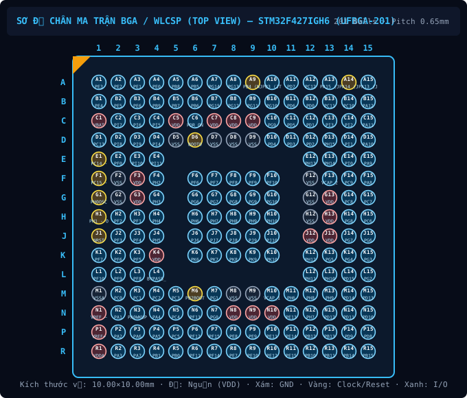
2. Standard-Pinbelegung (Draufsicht)CLEANROOM PINOUT
STM32F427IGH6 (UFBGA-201) - 2. Standard-Pinbelegung (Draufsicht)
Konforme Pinanordnung (201 Pins)Vergrößern ›
3. Original-Datenblatt-PinoutPDF PINOUT
STM32F427IGH6 (UFBGA-201) - 3. Original-Datenblatt-Pinout
Unbeschnittenes DatenblattdiagrammVergrößern ›
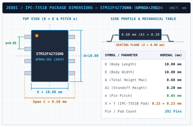
4. Gehäuseabmessungen (D×E×A)PACKAGE DIMENSIONS
STM32F427IGH6 (UFBGA-201) - 4. Gehäuseabmessungen (D×E×A)
UFBGA-201 · 10.00×10.00mm · Raster 0.65mmVergrößern ›
5. Empfohlener PCB-FootprintLAND PATTERN
STM32F427IGH6 (UFBGA-201) - 5. Empfohlener PCB-Footprint
IPC-7351B Land Pattern (201 Pads)Vergrößern ›
6. Typische ApplikationsschaltungSCHEMATIC
STM32F427IGH6 (UFBGA-201) - 6. Typische Applikationsschaltung
Typical Application SchematicVergrößern ›
Originale Datenblatt-Pinouts & Technische Zeichnungen (12 Abb. · Seite 1/1)
Zeige 1–12 von 12 unbeschnittenen Originalzeichnungen für STM32F429 / STM32F427
P1 · p01_fig01EXAKTES GEHÄUSE
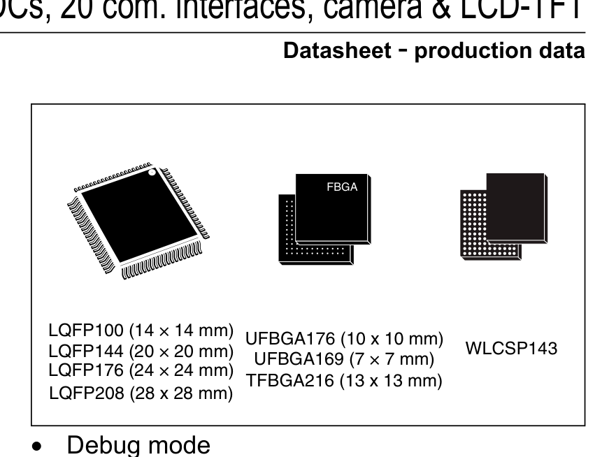
STM32F427IGH6 (UFBGA-201) — 32b Arm® Cortex®-M4 MCU+FPU, 225DMIPS, up to 2MB Flash/256+4KB RAM, USB OTG HS/FS, Ethernet, 17 TIMs, 3 ADCs, 20 com. interfaces, camera & LCD-TFT | Datasheet - production data | LQFP100 (14 × 14 mm) LQFP144 (20 × 20 mm) UFBGA176 (10 x 10 m
32b Arm® Cortex®-M4 MCU+FPU, 225DMIPS, up to 2MB Flash/256+4KB RAM, USB OTG HS/FS, Ethernet, 17 TIMs, 3 ADCs, 20 com. interfaces, camera & LCD-TFT | Datasheet - production data | LQFP100 (14 × 14 mm) LQFP144 (20 × 20 mm) UFBGA176 (10 x 10 m
P51 · p51_fig01EXAKTES GEHÄUSE
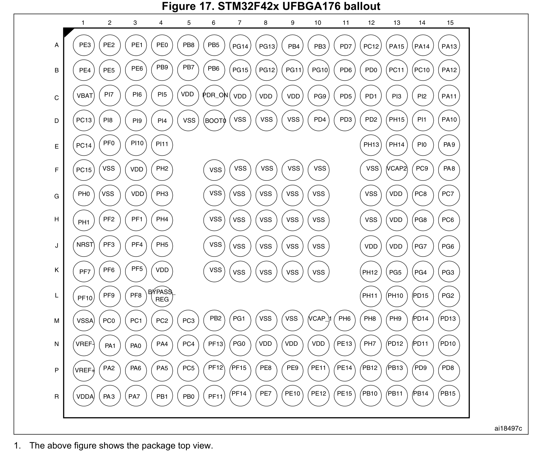
STM32F427IGH6 (UFBGA-201) — Figure 17. STM32F42x UFBGA176 ballout     
Figure 17. STM32F42x UFBGA176 ballout     
P221 · p221_fig01EXAKTES GEHÄUSE
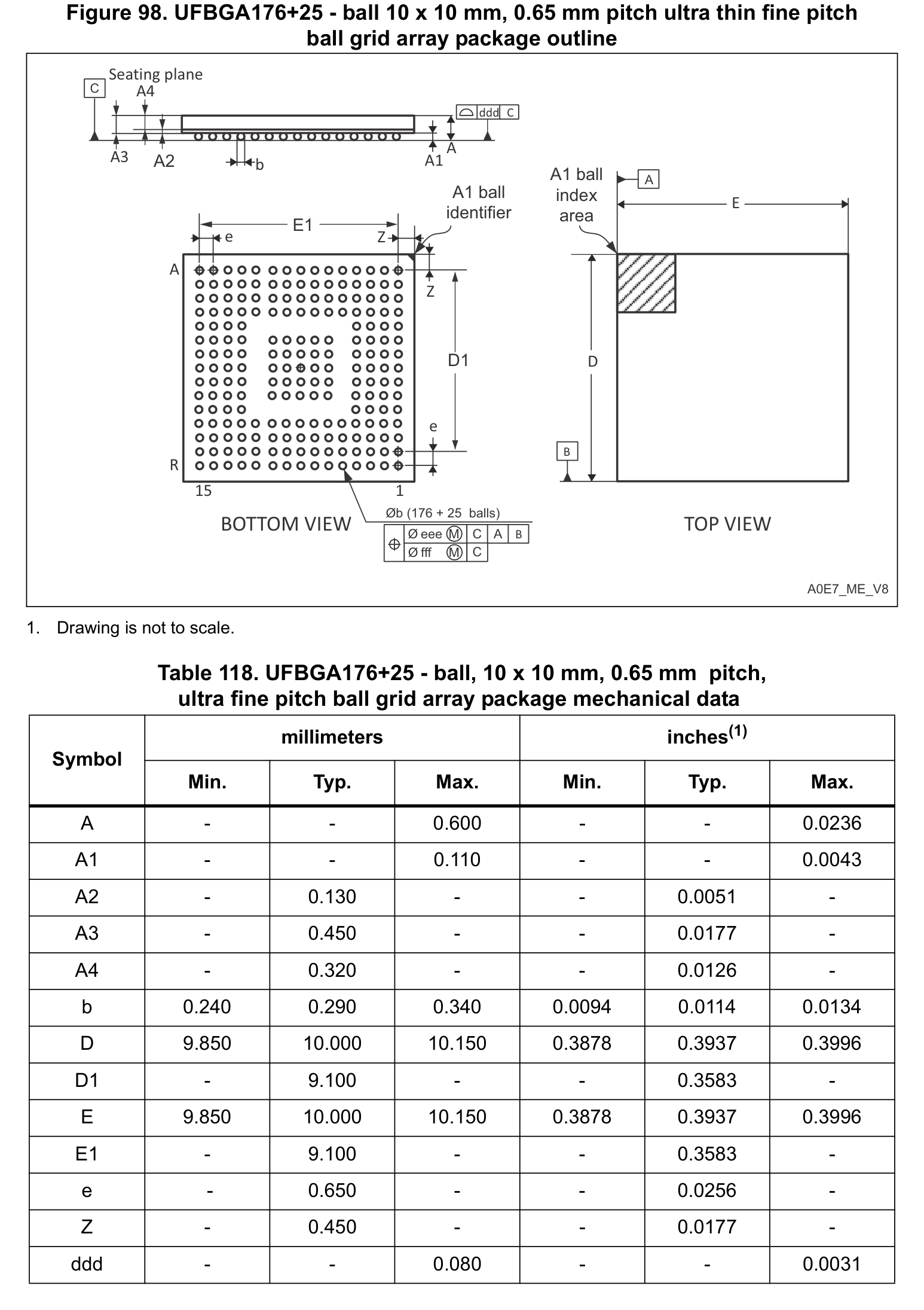
STM32F427IGH6 (UFBGA-201) — Figure 98. UFBGA176+25 - ball 10 x 10 mm, 0.65 mm pitch ultra thin fine pitch
Figure 98. UFBGA176+25 - ball 10 x 10 mm, 0.65 mm pitch ultra thin fine pitch
P222 · p222_fig01EXAKTES GEHÄUSE
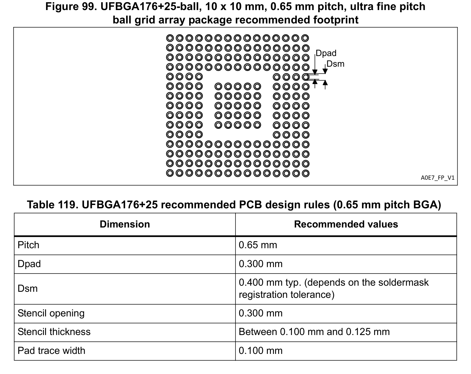
STM32F427IGH6 (UFBGA-201) — Figure 99. UFBGA176+25-ball, 10 x 10 mm, 0.65 mm pitch, ultra fine pitch
Figure 99. UFBGA176+25-ball, 10 x 10 mm, 0.65 mm pitch, ultra fine pitch
P45 · p45_fig011546×1419px
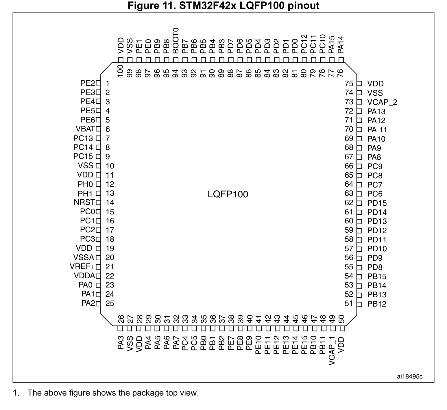
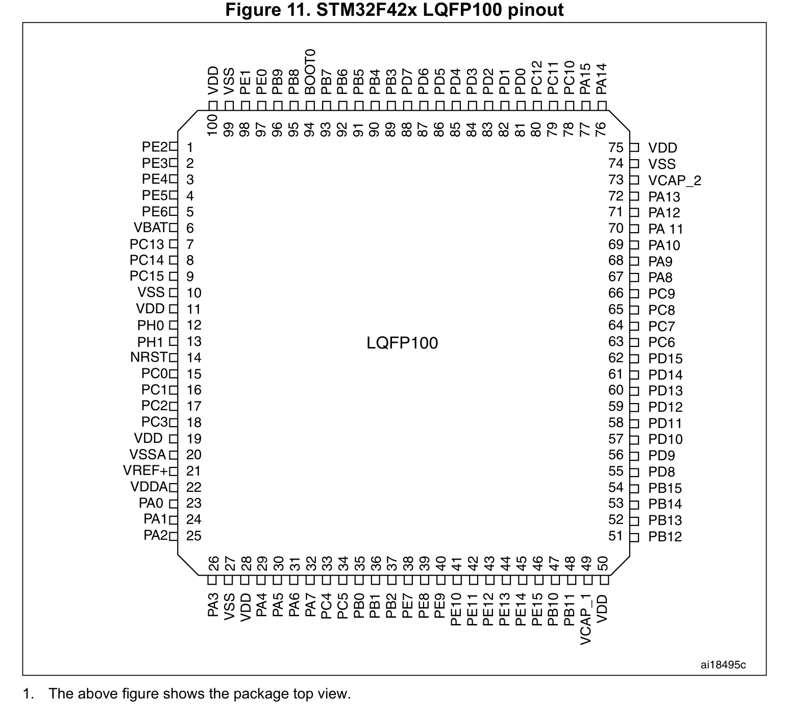
STM32F427IGH6 (UFBGA-201) — Figure 11. STM32F42x LQFP100 pinout 6$$ 633 0%�� 0%�� 0"�� 0"�� "//4��                          
Figure 11. STM32F42x LQFP100 pinout 6$$ 633 0% 0% 0" 0" "//4                          
P45 · p45_fig01P45
STM32F427IGH6 (UFBGA-201) — Datasheet Page 45 (p45_fig01)
Datasheet Page 45 (p45_fig01)
P92 · p92_fig011751×1451px
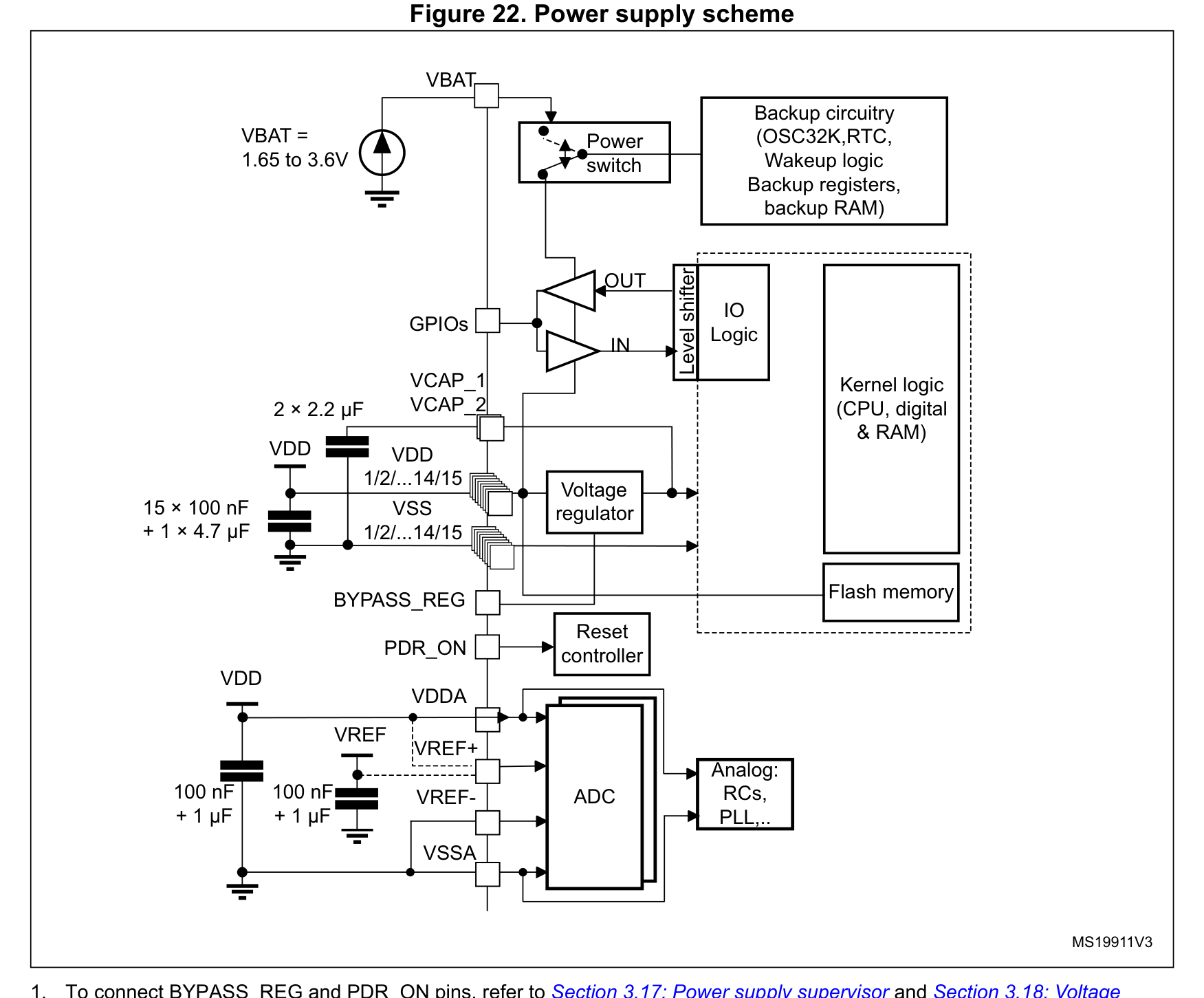
STM32F427IGH6 (UFBGA-201) — Figure 22. Power supply scheme 9%$7
Figure 22. Power supply scheme 9%$7
P219 · p219_fig011546×1121px
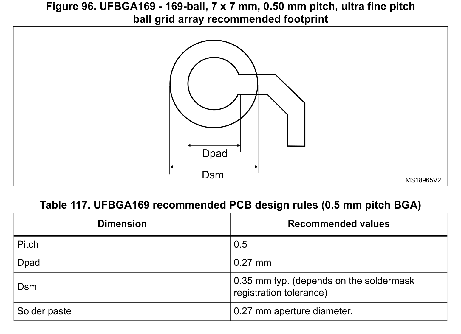
STM32F427IGH6 (UFBGA-201) — Figure 96. UFBGA169 - 169-ball, 7 x 7 mm, 0.50 mm pitch, ultra fine pitch
Figure 96. UFBGA169 - 169-ball, 7 x 7 mm, 0.50 mm pitch, ultra fine pitch
P221 · p221_fig01P221
STM32F427IGH6 (UFBGA-201) — Datasheet Page 221 (p221_fig01)
Datasheet Page 221 (p221_fig01)
P237 · p237_fig011548×2206px
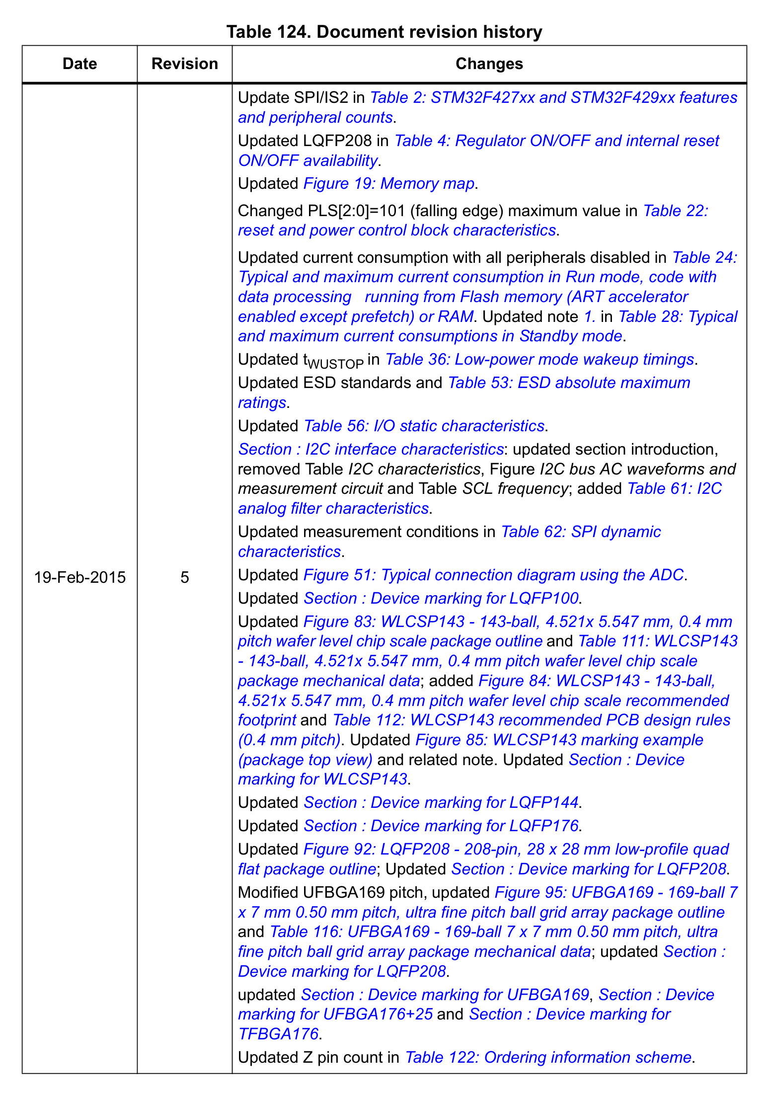
STM32F427IGH6 (UFBGA-201) — Revision history STM32F427xx STM32F429xx
Revision history STM32F427xx STM32F429xx
P238 · p238_fig011875×2535px
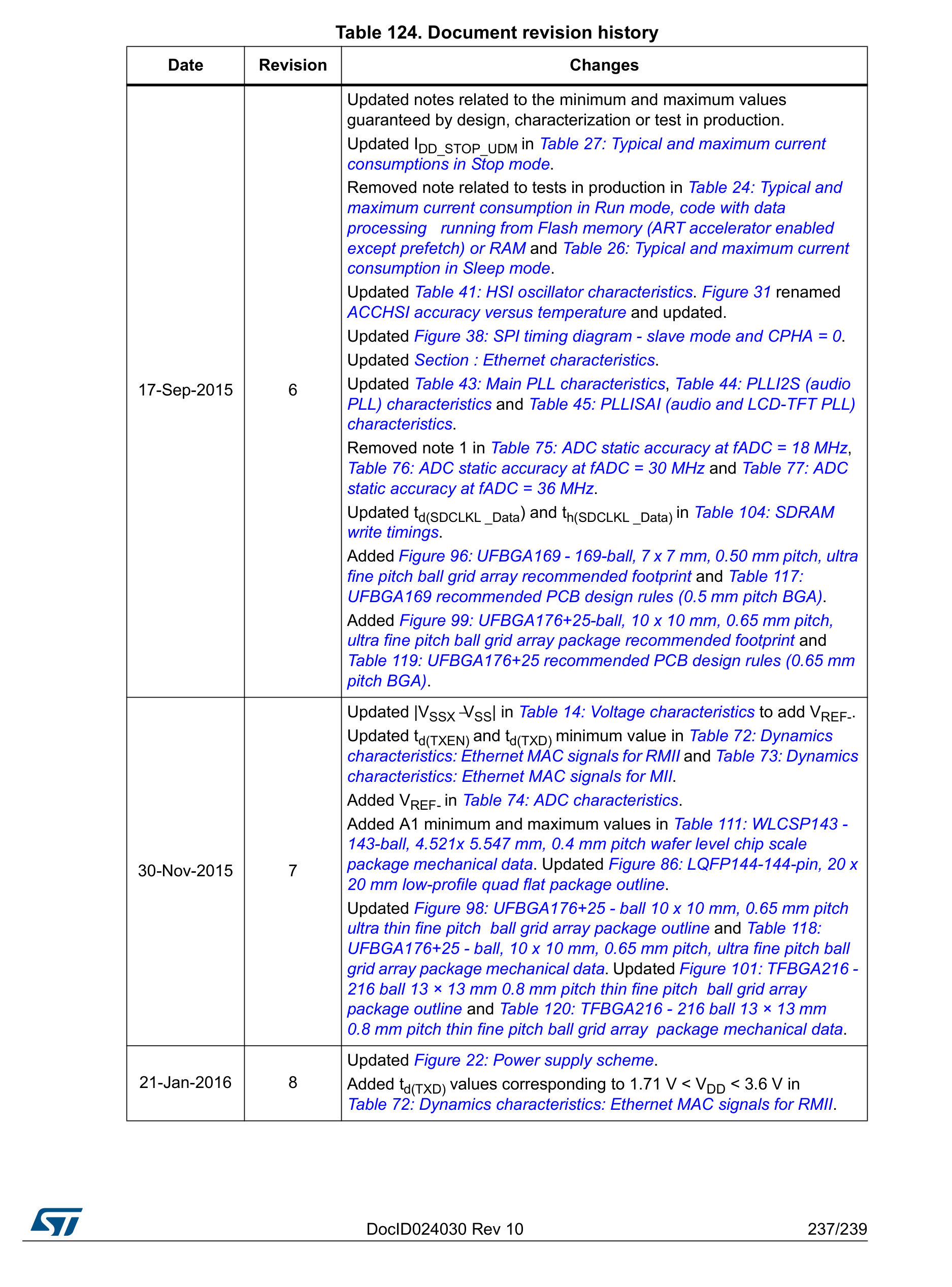
STM32F427IGH6 (UFBGA-201) — STM32F427xx STM32F429xx Revision history
STM32F427xx STM32F429xx Revision history
P238 · p238_fig01P238
STM32F427IGH6 (UFBGA-201) — Datasheet Page 238 (p238_fig01)
Datasheet Page 238 (p238_fig01)

Elektrische Spezifikationen & Bauteildetails (STM32F427IGH6)

Automatisch aus dem Datenblatt extrahierte Funktionsbeschreibung, Abmessungen, Betriebsspannungsbereich und Schnittstellen (DE)
Eingebetteter Mikrocontroller (MCU)
Detaillierte Übersicht:STM32F427IGH6 (UFBGA-201) ist ein 201-poliges Eingebetteter Mikrocontroller (MCU) mit den Gehäuseabmessungen 10.00 × 10.00 × 0.60 mm (Pin-Raster e = 0.65 mm). Ausgelegt für 1.7 V to 3.6 V Versorgungsspannung, -40°C ~ +85°C (Industrial Grade) Temperaturbereich und USB, I2C, I2S, ADC, PWM, SDIO, JTAG / SWD, IrDA, CAN, DAC, RTC/CLK, SPI, SWD/JTAG, UART Schnittstellen.
BetriebsversorgungsspannungV_CC / V_DD
1.7 V to 3.6 V
100nF + 10µF X7R Stützkondensatoren < 2mm am Versorgungspin platzieren
UmgebungstemperaturbereichT_A
-40°C ~ +85°C (Industrial Grade)
Industrieller Temperaturbereich; T_J(max) = +125°C
Takt- & Funkfrequenzf_CLK / f_RF
180 MHz
Aus offiziellen PDF-Datenblatttabellen extrahiert
Strom- & LeistungsdatenI_OUT / I_CC
I_GPIO(max) = ±20 mA / pin | I_VDD(total) ≤ 150 mA
139 5V-tolerante (FT) Pins erkannt
Gehäuseabmessungen (D × E × A)D × E × A
10.00 × 10.00 × 0.60 mm (A1=0.20 mm)
Gehäusefamilie: BGA (UFBGA-201)
Pinanzahl & RastermaßN / e
201 Pins | Pitch e = 0.65 mm (25.6 mil)
Nach IPC-7351B Mittenabstand C normalisiert
Integrierte BusschnittstellenBuses
USB, I2C, I2S, ADC, PWM, SDIO, JTAG / SWD, IrDA, CAN, DAC, RTC/CLK, SPI, SWD/JTAG, UART
4-Wege-Synchronisation (Symbol ↔ Pinout ↔ 2D ↔ 3D)
Lötprofil & FeuchteempfindlichkeitIPC / MSL
IPC-7351B Level B | J-STD-020 (Peak 260°C) | MSL-3
60% Pastenmasken-Segmentierung auf dem Thermal-Pad
Technischer Sicherheitshinweis: Boot-Strapping-Pin-Warnung (BOOT0, PB2BOOT1 - (PB2)): Keine störenden externen Pull-Ups/Pull-Downs während des Power-On-Resets beschalten.
Technischer Sicherheitshinweis: Thermal-Pad über Ø0.3mm Thermodurchkontaktierungen niederimpedant an die GND-Lage anbinden.

5-Punkte-Industriestandardprüfung

Automatische Geometrie- und Regelprüfung vor dem Dateiexport
5/5 BESTANDEN
IEEE-315 Symbol201 Pins automatisch nach Bussen gruppiert
OK
IPC-7351B Footprint201 Pads · Raster 0.65mm
OK
IPC-7525 60% LotpastenfensterReflow 1:1 Standard
OK
DFM-Fertigungsregeln (JLCPCB / PCBWay)Min. Pad-Abstand: 0.25mm
OK
3D STEP AP214 & GLBKoordinatenursprung deckungsgleich (0,0,0)
OK

Praxisverifikation & Ingenieurbewertungen

Automatisch aus dem Datenblatt extrahierte Funktionsbeschreibung, Abmessungen, Betriebsspannungsbereich und Schnittstellen
5.00 PCB Verified

Mechanische Abmessungen & Land Pattern (UFBGA-201)

Aus dem Datenblatt extrahiert & nach IPC-7351B normiert
mm
Gehäusekörper (D × E)Nominal
10.00 × 10.00 mm
Höhe (A) & Raster (e)IPC-7351B
A=0.60mm · e=0.65mm
Pad-Abmessungen (W × L)Level B
0.23 × 0.23 mm
Pins / Gesamt-PadsTopology
201P / 201Pad (BGA_GRID)

Empfohlene Peripherie-BOM & Pin-kompatible Ersatztypen (Drop-in)

Passive Begleitbauteile gemäß Referenzschaltung sowie 1:1 pin-kompatible Alternativen
DFM READY
Bauteilbezeichner / Ersatz-MPNWert / GehäuseFunktion & PCB-Layout-Regel
N/A
BOM
Gemäß Applikationsschaltung
UFBGA-201
Leiterbahnbreiten für Nennstrom dimensionieren und IPC-2221 Isolationsabstände einhalten.

Häufig gestellte technische Fragen (FAQ) — STM32F427IGH6 (UFBGA-201)

Schnellantworten zu Pinbelegung, IPC-7351B Land-Pattern-Abmessungen und CAD-Exportformaten
IPC-7351B / IEEE-315

Wie lautet die Pinbelegung (Pinout) und Versorgungsspannung des STM32F427IGH6 (UFBGA-201)?

Das Bauteil STM32F427IGH6 von ST im UFBGA-201-Gehäuse besitzt 201 Pins mit einem Rastermaß (Pitch) von 0.65 mm und einem Betriebsspannungsbereich VCC von 1.7 V to 3.6 V. Wichtige Pins: A1 (PE3: Multiplex-I/O- & Peripherie-Pin PE3 (General)), A2 (PE2: Multiplex-I/O- & Peripherie-Pin PE2 (SPI)), A3 (PE1: Multiplex-I/O- & Peripherie-Pin PE1 (UART)), A4 (PE0: Multiplex-I/O- & Peripherie-Pin PE0 (UART)), A5 (PB8: Multiplex-I/O- & Peripherie-Pin PB8 (I2C, PWM)), A6 (PB5: Multiplex-I/O- & Peripherie-Pin PB5 (SPI, I2C, PWM, CAN)).

Welche IPC-7351B Land-Pattern-Abmessungen hat der STM32F427IGH6?

Gemäß Datenblatt und IPC-7351B (Density Level B Nominal) betragen die Gehäusemaße des STM32F427IGH6 (UFBGA-201) 10.00 × 10.00 mm bei einem Pitch e = 0.65 mm und 201 Kupfer-Pads.

Wo können KiCad (.kicad_mod, .kicad_sym), Fusion 360 (.lbr) und 3D-STEP-Modelle für STM32F427IGH6 heruntergeladen werden?

Auf dieser Seite können Sie das vollständig verifizierte CAD-Bibliothekspaket für STM32F427IGH6 (ST, UFBGA-201) unter der Open-Hardware-Lizenz CERN-OHL-P-2.0 kostenlos herunterladen: KiCad 8 Footprint (.kicad_mod), Schaltplansymbol (.kicad_sym), Fusion 360 / Eagle (.lbr) und 3D STEP AP214 / WebGL GLB.

Statischer Referenzanhang: Pinbelegungstabelle (201 Pins) & STM32F429 / STM32F427 VariantenStatische Tabelle aufklappen
Pin-Nr.SignalnameElektrischer TypFunktionsbeschreibung & Schaltungshinweise
A1PE3Digital_IOSignalanschluss PE3 (Richtung: I/O, Spannungsbereich: 3.3V VDD (5V-Tolerant FT)). Alternative Multiplex-Funktionen: PE3. Unterstützte Bus-Schnittstellen: General.
A2PE2Digital_IOSignalanschluss PE2 (Richtung: I/O, Spannungsbereich: 3.3V VDD (5V-Tolerant FT)). Alternative Multiplex-Funktionen: SPI4_SCK. Unterstützte Bus-Schnittstellen: SPI.
A3PE1Digital_IOSignalanschluss PE1 (Richtung: I/O, Spannungsbereich: 3.3V VDD (5V-Tolerant FT)). Alternative Multiplex-Funktionen: PE1. Unterstützte Bus-Schnittstellen: UART.
A4PE0Digital_IOSignalanschluss PE0 (Richtung: I/O, Spannungsbereich: 3.3V VDD (5V-Tolerant FT)). Alternative Multiplex-Funktionen: PE0. Unterstützte Bus-Schnittstellen: UART.
A5PB8Digital_IOSignalanschluss PB8 (Richtung: I/O, Spannungsbereich: 3.3V VDD (5V-Tolerant FT)). Alternative Multiplex-Funktionen: PB8. Unterstützte Bus-Schnittstellen: I2C, PWM.
A6PB5Digital_IOSignalanschluss PB5 (Richtung: I/O, Spannungsbereich: 3.3V VDD (5V-Tolerant FT)). Alternative Multiplex-Funktionen: I2C1_SMBA, SPI1_MOSI, SPI3_MOSI. Unterstützte Bus-Schnittstellen: SPI, I2C, PWM, CAN.
A7PG14Digital_IOSignalanschluss PG14 (Richtung: I/O, Spannungsbereich: 3.3V VDD (5V-Tolerant FT)). Alternative Multiplex-Funktionen: SPI6_MOSI. Unterstützte Bus-Schnittstellen: UART, SPI.
A8PG13Digital_IOSignalanschluss PG13 (Richtung: I/O, Spannungsbereich: 3.3V VDD (5V-Tolerant FT)). Alternative Multiplex-Funktionen: SPI6_SCK. Unterstützte Bus-Schnittstellen: UART, SPI.
A9PB4 (NJTRST)Digital_IOSignalanschluss PB4 (NJTRST) (Richtung: I/O, Spannungsbereich: 3.3V VDD (5V-Tolerant FT)). Alternative Multiplex-Funktionen: SPI1_MISO, SPI3_MISO. Unterstützte Bus-Schnittstellen: SPI, SWD/JTAG.
A10PB3 (JTDO/TRACE SWO)Digital_IOSignalanschluss PB3 (JTDO/TRACE SWO) (Richtung: I/O, Spannungsbereich: 3.3V VDD (5V-Tolerant FT)). Alternative Multiplex-Funktionen: SPI3_SCK. Unterstützte Bus-Schnittstellen: SPI, PWM, SWD/JTAG.
A11PD7Digital_IOSignalanschluss PD7 (Richtung: I/O, Spannungsbereich: 3.3V VDD (5V-Tolerant FT)). Alternative Multiplex-Funktionen: PD7. Unterstützte Bus-Schnittstellen: UART.
A12PC12Digital_IOSignalanschluss PC12 (Richtung: I/O, Spannungsbereich: 3.3V VDD (5V-Tolerant FT)). Alternative Multiplex-Funktionen: SPI3_MOSI. Unterstützte Bus-Schnittstellen: UART, SPI.
A13PA15 (JTDI)Digital_IOSignalanschluss PA15 (JTDI) (Richtung: I/O, Spannungsbereich: 3.3V VDD (5V-Tolerant FT)). Alternative Multiplex-Funktionen: SPI1_NSS, SPI3_NSS. Unterstützte Bus-Schnittstellen: SPI, SWD/JTAG.
A14PA14 (JTCK - SWCLK)Digital_IOSignalanschluss PA14 (JTCK - SWCLK) (Richtung: I/O, Spannungsbereich: 3.3V VDD (5V-Tolerant FT)). Alternative Multiplex-Funktionen: PA14 (JTCK - SWCLK). Unterstützte Bus-Schnittstellen: SWD/JTAG.
A15PA13 (JTMS - SWDIO)Digital_IOSignalanschluss PA13 (JTMS - SWDIO) (Richtung: I/O, Spannungsbereich: 3.3V VDD (5V-Tolerant FT)). Alternative Multiplex-Funktionen: PA13 (JTMS - SWDIO). Unterstützte Bus-Schnittstellen: SWD/JTAG.
B1PE4Digital_IOSignalanschluss PE4 (Richtung: I/O, Spannungsbereich: 3.3V VDD (5V-Tolerant FT)). Alternative Multiplex-Funktionen: SPI4_NSS. Unterstützte Bus-Schnittstellen: SPI.
B2PE5Digital_IOSignalanschluss PE5 (Richtung: I/O, Spannungsbereich: 3.3V VDD (5V-Tolerant FT)). Alternative Multiplex-Funktionen: SPI4_MISO. Unterstützte Bus-Schnittstellen: SPI.
B3PE6Digital_IOSignalanschluss PE6 (Richtung: I/O, Spannungsbereich: 3.3V VDD (5V-Tolerant FT)). Alternative Multiplex-Funktionen: SPI4_MOSI. Unterstützte Bus-Schnittstellen: SPI.
B4PB9Digital_IOSignalanschluss PB9 (Richtung: I/O, Spannungsbereich: 3.3V VDD (5V-Tolerant FT)). Alternative Multiplex-Funktionen: I2C1_SDA, SPI2_NSS. Unterstützte Bus-Schnittstellen: SPI, I2C, PWM, CAN.
B5PB7Digital_IOSignalanschluss PB7 (Richtung: I/O, Spannungsbereich: 3.3V VDD (5V-Tolerant FT)). Alternative Multiplex-Funktionen: PB7. Unterstützte Bus-Schnittstellen: UART, PWM.
B6PB6Digital_IOSignalanschluss PB6 (Richtung: I/O, Spannungsbereich: 3.3V VDD (5V-Tolerant FT)). Alternative Multiplex-Funktionen: PB6. Unterstützte Bus-Schnittstellen: UART, PWM, CAN.
B7PG15Digital_IOSignalanschluss PG15 (Richtung: I/O, Spannungsbereich: 3.3V VDD (5V-Tolerant FT)). Alternative Multiplex-Funktionen: PG15. Unterstützte Bus-Schnittstellen: UART.
B8PG12Digital_IOSignalanschluss PG12 (Richtung: I/O, Spannungsbereich: 3.3V VDD (5V-Tolerant FT)). Alternative Multiplex-Funktionen: SPI6_MISO. Unterstützte Bus-Schnittstellen: UART, SPI.
B9PG11Digital_IOSignalanschluss PG11 (Richtung: I/O, Spannungsbereich: 3.3V VDD (5V-Tolerant FT)). Alternative Multiplex-Funktionen: PG11. Unterstützte Bus-Schnittstellen: General.
B10PG10Digital_IOSignalanschluss PG10 (Richtung: I/O, Spannungsbereich: 3.3V VDD (5V-Tolerant FT)). Alternative Multiplex-Funktionen: PG10. Unterstützte Bus-Schnittstellen: General.
B11PD6Digital_IOSignalanschluss PD6 (Richtung: I/O, Spannungsbereich: 3.3V VDD (5V-Tolerant FT)). Alternative Multiplex-Funktionen: SPI3_MOSI. Unterstützte Bus-Schnittstellen: UART, SPI, I2C.
B12PD0Digital_IOSignalanschluss PD0 (Richtung: I/O, Spannungsbereich: 3.3V VDD (5V-Tolerant FT)). Alternative Multiplex-Funktionen: PD0. Unterstützte Bus-Schnittstellen: CAN.
B13PC11Digital_IOSignalanschluss PC11 (Richtung: I/O, Spannungsbereich: 3.3V VDD (5V-Tolerant FT)). Alternative Multiplex-Funktionen: SPI3_MISO. Unterstützte Bus-Schnittstellen: UART, SPI.
B14PC10Digital_IOSignalanschluss PC10 (Richtung: I/O, Spannungsbereich: 3.3V VDD (5V-Tolerant FT)). Alternative Multiplex-Funktionen: SPI3_SCK. Unterstützte Bus-Schnittstellen: UART, SPI.
B15PA12Digital_IOSignalanschluss PA12 (Richtung: I/O, Spannungsbereich: 3.3V VDD (5V-Tolerant FT)). Alternative Multiplex-Funktionen: PA12. Unterstützte Bus-Schnittstellen: UART, CAN.
C1VBATPower_InPositiver Versorgungseingang (VBAT) im Spannungsbereich 3.3V VDD (Max 4.0V) (Max. 4.0V).
C2PI7Digital_IOSignalanschluss PI7 (Richtung: I/O, Spannungsbereich: 3.3V VDD (5V-Tolerant FT)). Alternative Multiplex-Funktionen: PI7. Unterstützte Bus-Schnittstellen: PWM.
C3PI6Digital_IOSignalanschluss PI6 (Richtung: I/O, Spannungsbereich: 3.3V VDD (5V-Tolerant FT)). Alternative Multiplex-Funktionen: PI6. Unterstützte Bus-Schnittstellen: PWM.
C4PI5Digital_IOSignalanschluss PI5 (Richtung: I/O, Spannungsbereich: 3.3V VDD (5V-Tolerant FT)). Alternative Multiplex-Funktionen: PI5. Unterstützte Bus-Schnittstellen: PWM.
C5VDDPower_InPositiver Versorgungseingang (VDD) im Spannungsbereich 3.3V VDD (Max 4.0V) (Max. 4.0V).
C6PDR_ONDigital_IOSignalanschluss PDR_ON (Richtung: I/O, Spannungsbereich: 3.3V VDD (Max 4.0V)). Alternative Multiplex-Funktionen: PDR_ON. Unterstützte Bus-Schnittstellen: General.
C7VDDPower_InPositiver Versorgungseingang (VDD) im Spannungsbereich 3.3V VDD (Max 4.0V) (Max. 4.0V).
C8VDDPower_InPositiver Versorgungseingang (VDD) im Spannungsbereich 3.3V VDD (Max 4.0V) (Max. 4.0V).
C9VDDPower_InPositiver Versorgungseingang (VDD) im Spannungsbereich 3.3V VDD (Max 4.0V) (Max. 4.0V).
C10PG9Digital_IOSignalanschluss PG9 (Richtung: I/O, Spannungsbereich: 3.3V VDD (5V-Tolerant FT)). Alternative Multiplex-Funktionen: PG9. Unterstützte Bus-Schnittstellen: UART.
C11PD5Digital_IOSignalanschluss PD5 (Richtung: I/O, Spannungsbereich: 3.3V VDD (5V-Tolerant FT)). Alternative Multiplex-Funktionen: PD5. Unterstützte Bus-Schnittstellen: UART.
C12PD1Digital_IOSignalanschluss PD1 (Richtung: I/O, Spannungsbereich: 3.3V VDD (5V-Tolerant FT)). Alternative Multiplex-Funktionen: PD1. Unterstützte Bus-Schnittstellen: CAN.
C13PI3Digital_IOSignalanschluss PI3 (Richtung: I/O, Spannungsbereich: 3.3V VDD (5V-Tolerant FT)). Alternative Multiplex-Funktionen: SPI2_MOSI. Unterstützte Bus-Schnittstellen: SPI.
C14PI2Digital_IOSignalanschluss PI2 (Richtung: I/O, Spannungsbereich: 3.3V VDD (5V-Tolerant FT)). Alternative Multiplex-Funktionen: SPI2_MISO. Unterstützte Bus-Schnittstellen: SPI, PWM.
C15PA11Digital_IOSignalanschluss PA11 (Richtung: I/O, Spannungsbereich: 3.3V VDD (5V-Tolerant FT)). Alternative Multiplex-Funktionen: PA11. Unterstützte Bus-Schnittstellen: UART, PWM, CAN.
D1PC13Digital_IOSignalanschluss PC13 (Richtung: I/O, Spannungsbereich: 3.3V VDD (5V-Tolerant FT)). Alternative Multiplex-Funktionen: PC13. Unterstützte Bus-Schnittstellen: General.
D2PI8Digital_IOSignalanschluss PI8 (Richtung: I/O, Spannungsbereich: 3.3V VDD (5V-Tolerant FT)). Alternative Multiplex-Funktionen: PI8. Unterstützte Bus-Schnittstellen: General.
D3PI9Digital_IOSignalanschluss PI9 (Richtung: I/O, Spannungsbereich: 3.3V VDD (5V-Tolerant FT)). Alternative Multiplex-Funktionen: PI9. Unterstützte Bus-Schnittstellen: CAN.
D4PI4Digital_IOSignalanschluss PI4 (Richtung: I/O, Spannungsbereich: 3.3V VDD (5V-Tolerant FT)). Alternative Multiplex-Funktionen: PI4. Unterstützte Bus-Schnittstellen: General.
D5VSSGNDElektrischer 0V-Masserückführungsanschluss (VSS) für Kernlogik, I/O-Treiber und Analogblöcke.
D6BOOT0Digital_IOSignalanschluss BOOT0 (Richtung: I, Spannungsbereich: 3.3V VDD (Max 4.0V)). Alternative Multiplex-Funktionen: BOOT0. Unterstützte Bus-Schnittstellen: General.
D7VSSGNDElektrischer 0V-Masserückführungsanschluss (VSS) für Kernlogik, I/O-Treiber und Analogblöcke.
D8VSSGNDElektrischer 0V-Masserückführungsanschluss (VSS) für Kernlogik, I/O-Treiber und Analogblöcke.
D9VSSGNDElektrischer 0V-Masserückführungsanschluss (VSS) für Kernlogik, I/O-Treiber und Analogblöcke.
D10PD4Digital_IOSignalanschluss PD4 (Richtung: I/O, Spannungsbereich: 3.3V VDD (5V-Tolerant FT)). Alternative Multiplex-Funktionen: PD4. Unterstützte Bus-Schnittstellen: UART.
D11PD3Digital_IOSignalanschluss PD3 (Richtung: I/O, Spannungsbereich: 3.3V VDD (5V-Tolerant FT)). Alternative Multiplex-Funktionen: SPI2_SCK. Unterstützte Bus-Schnittstellen: UART, SPI.
D12PD2Digital_IOSignalanschluss PD2 (Richtung: I/O, Spannungsbereich: 3.3V VDD (5V-Tolerant FT)). Alternative Multiplex-Funktionen: PD2. Unterstützte Bus-Schnittstellen: UART.
D13PH15Digital_IOSignalanschluss PH15 (Richtung: I/O, Spannungsbereich: 3.3V VDD (5V-Tolerant FT)). Alternative Multiplex-Funktionen: PH15. Unterstützte Bus-Schnittstellen: PWM.
D14PI1Digital_IOSignalanschluss PI1 (Richtung: I/O, Spannungsbereich: 3.3V VDD (5V-Tolerant FT)). Alternative Multiplex-Funktionen: SPI2_SCK. Unterstützte Bus-Schnittstellen: SPI.
D15PA10Digital_IOSignalanschluss PA10 (Richtung: I/O, Spannungsbereich: 3.3V VDD (5V-Tolerant FT)). Alternative Multiplex-Funktionen: PA10. Unterstützte Bus-Schnittstellen: UART, PWM.
E1PC14 - OSC32_IN (PC14)Digital_IOSignalanschluss PC14 - OSC32_IN (PC14) (Richtung: I/O, Spannungsbereich: 3.3V VDD (5V-Tolerant FT)). Alternative Multiplex-Funktionen: PC14 - OSC32_IN (PC14). Unterstützte Bus-Schnittstellen: RTC/CLK.
E2PF0Digital_IOSignalanschluss PF0 (Richtung: I/O, Spannungsbereich: 3.3V VDD (5V-Tolerant FT)). Alternative Multiplex-Funktionen: PF0. Unterstützte Bus-Schnittstellen: I2C.
E3PI10Digital_IOSignalanschluss PI10 (Richtung: I/O, Spannungsbereich: 3.3V VDD (5V-Tolerant FT)). Alternative Multiplex-Funktionen: PI10. Unterstützte Bus-Schnittstellen: General.
E4PI11Digital_IOSignalanschluss PI11 (Richtung: I/O, Spannungsbereich: 3.3V VDD (5V-Tolerant FT)). Alternative Multiplex-Funktionen: PI11. Unterstützte Bus-Schnittstellen: General.