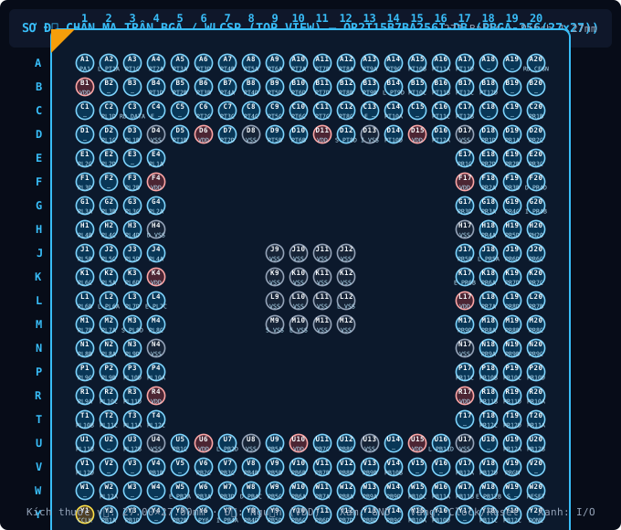
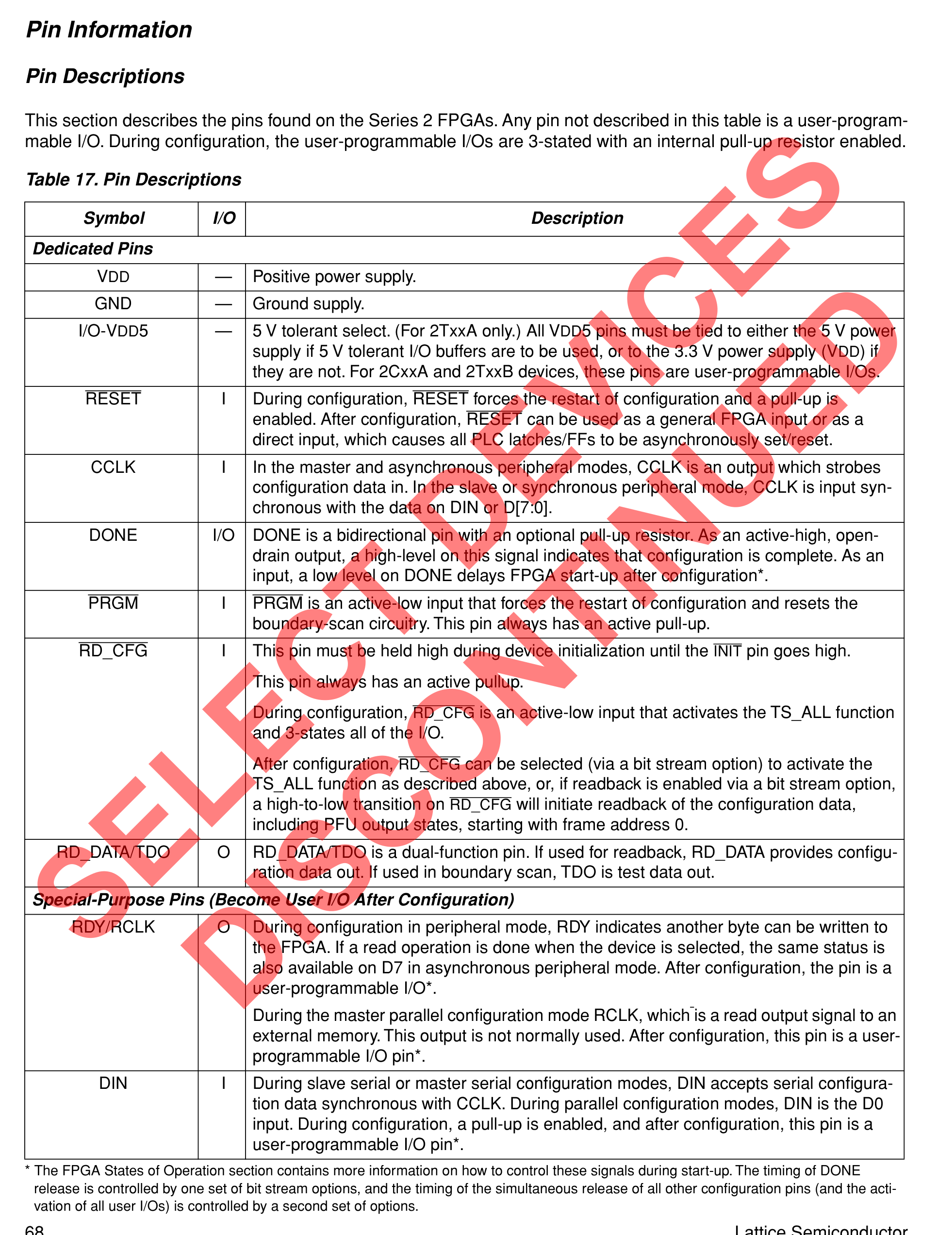
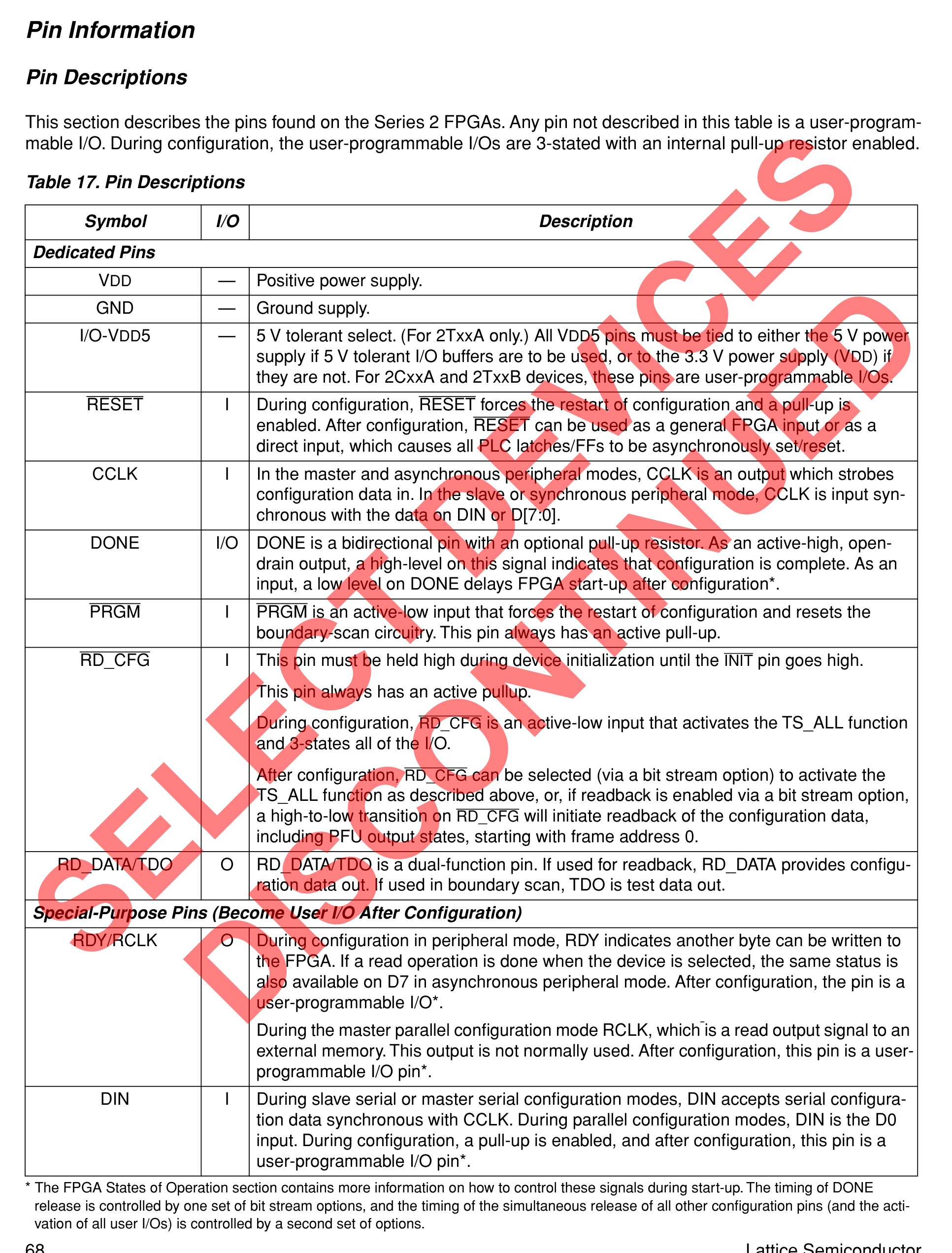
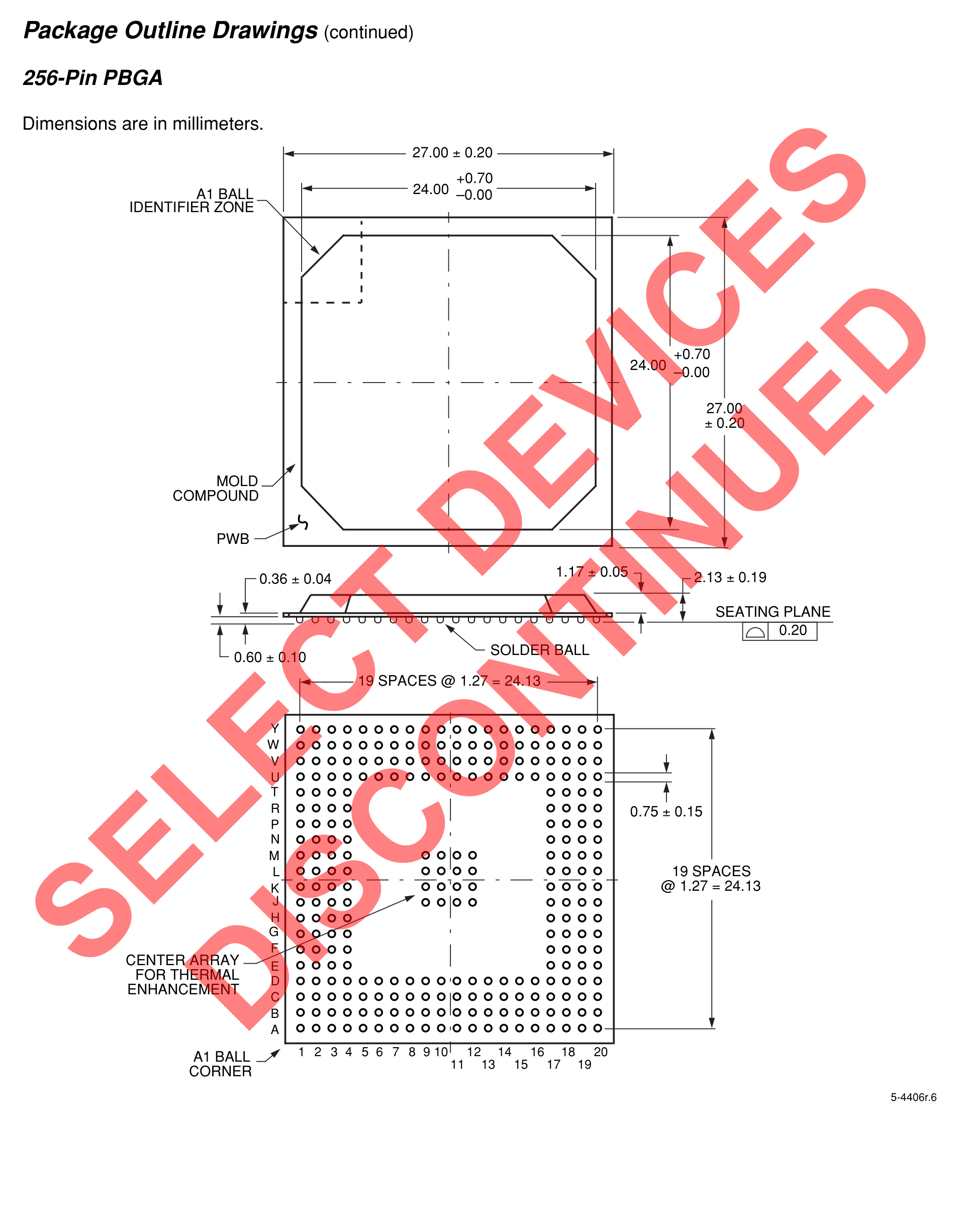
| A1 | PA1 | I/O | Multiplexed I/O & Peripheral Pin PA1 (General) |
| A2 | L PT1A | I/O | Multiplexed I/O & Peripheral Pin L PT1A (General) |
| A3 | PT1C | I/O | Multiplexed I/O & Peripheral Pin PT1C (General) |
| A4 | PT2A | I/O | Multiplexed I/O & Peripheral Pin PT2A (General) |
| A5 | PT3A | I/O | Multiplexed I/O & Peripheral Pin PT3A (General) |
| A6 | PT3D | I/O | Multiplexed I/O & Peripheral Pin PT3D (General) |
| A7 | PT4B | I/O | Multiplexed I/O & Peripheral Pin PT4B (General) |
| A8 | PT5A | I/O | Multiplexed I/O & Peripheral Pin PT5A (General) |
| A9 | PT6A | I/O | Multiplexed I/O & Peripheral Pin PT6A (General) |
| A10 | PT7A | I/O | Multiplexed I/O & Peripheral Pin PT7A (General) |
| A11 | PT7B | I/O | Multiplexed I/O & Peripheral Pin PT7B (General) |
| A12 | PT8A | I/O | Multiplexed I/O & Peripheral Pin PT8A (General) |
| A13 | PT9A | I/O | Multiplexed I/O & Peripheral Pin PT9A (General) |
| A14 | PT9C | I/O | Multiplexed I/O & Peripheral Pin PT9C (General) |
| A15 | PT10B | I/O | Multiplexed I/O & Peripheral Pin PT10B (General) |
| A16 | PT11A | I/O | Multiplexed I/O & Peripheral Pin PT11A (General) |
| A17 | PT11D | I/O | Multiplexed I/O & Peripheral Pin PT11D (General) |
| A18 | — | I/O | Multiplexed I/O & Peripheral Pin — (General) |
| A19 | — | I/O | Multiplexed I/O & Peripheral Pin — (General) |
| A20 | RD_CFGN | I/O | Multiplexed I/O & Peripheral Pin RD_CFGN (General) |
| B1 | VDD | Power | Power Supply Input (VDD — 3.0 V to 3.6 V) |
| B2 | — | I/O | Multiplexed I/O & Peripheral Pin — (General) |
| B3 | — | I/O | Multiplexed I/O & Peripheral Pin — (General) |
| B4 | PT1D | I/O | Multiplexed I/O & Peripheral Pin PT1D (General) |
| B5 | PT2B | I/O | Multiplexed I/O & Peripheral Pin PT2B (General) |
| B6 | PT3B | I/O | Multiplexed I/O & Peripheral Pin PT3B (General) |
| B7 | PT4A | I/O | Multiplexed I/O & Peripheral Pin PT4A (General) |
| B8 | PT4D | I/O | Multiplexed I/O & Peripheral Pin PT4D (General) |
| B9 | PT5D | I/O | Multiplexed I/O & Peripheral Pin PT5D (General) |
| B10 | PT6D | I/O | Multiplexed I/O & Peripheral Pin PT6D (General) |
| B11 | PT7D | I/O | Multiplexed I/O & Peripheral Pin PT7D (General) |
| B12 | PT8B | I/O | Multiplexed I/O & Peripheral Pin PT8B (General) |
| B13 | PT9B | I/O | Multiplexed I/O & Peripheral Pin PT9B (General) |
| B14 | L PT9D | I/O | Multiplexed I/O & Peripheral Pin L PT9D (General) |
| B15 | PT10C | I/O | Multiplexed I/O & Peripheral Pin PT10C (General) |
| B16 | PT11B | I/O | Multiplexed I/O & Peripheral Pin PT11B (General) |
| B17 | PT12C | I/O | Multiplexed I/O & Peripheral Pin PT12C (General) |
| B18 | PT12D | I/O | Multiplexed I/O & Peripheral Pin PT12D (General) |
| B19 | — | I/O | Multiplexed I/O & Peripheral Pin — (General) |
| B20 | — | I/O | Multiplexed I/O & Peripheral Pin — (General) |
| C1 | — | I/O | Multiplexed I/O & Peripheral Pin — (General) |
| C2 | PL1D | I/O | Multiplexed I/O & Peripheral Pin PL1D (General) |
| C3 | RD DATA/TDO_ | I/O | Multiplexed I/O & Peripheral Pin RD DATA/TDO_ (General) |
| C4 | E — | I/O | Multiplexed I/O & Peripheral Pin E — (General) |
| C5 | — | I/O | Multiplexed I/O & Peripheral Pin — (General) |
| C6 | PT2C | I/O | Multiplexed I/O & Peripheral Pin PT2C (General) |
| C7 | PT3C | I/O | Multiplexed I/O & Peripheral Pin PT3C (General) |
| C8 | PT4C | I/O | Multiplexed I/O & Peripheral Pin PT4C (General) |
| C9 | PT5C | I/O | Multiplexed I/O & Peripheral Pin PT5C (General) |
| C10 | PT6C | I/O | Multiplexed I/O & Peripheral Pin PT6C (General) |
| C11 | PT7C | I/O | Multiplexed I/O & Peripheral Pin PT7C (General) |
| C12 | PT8C | I/O | Multiplexed I/O & Peripheral Pin PT8C (General) |
| C13 | E — | I/O | Multiplexed I/O & Peripheral Pin E — (General) |
| C14 | PT10A | I/O | Multiplexed I/O & Peripheral Pin PT10A (General) |
| C15 | — | I/O | Multiplexed I/O & Peripheral Pin — (General) |
| C16 | PT11C | I/O | Multiplexed I/O & Peripheral Pin PT11C (General) |
| C17 | PT12B | I/O | Multiplexed I/O & Peripheral Pin PT12B (General) |
| C18 | — | I/O | Multiplexed I/O & Peripheral Pin — (General) |
| C19 | — | I/O | Multiplexed I/O & Peripheral Pin — (General) |
| C20 | PR1B | I/O | Multiplexed I/O & Peripheral Pin PR1B (General) |
| D1 | — | I/O | Multiplexed I/O & Peripheral Pin — (General) |
| D2 | PL1C | I/O | Multiplexed I/O & Peripheral Pin PL1C (General) |
| D3 | PL1B | I/O | Multiplexed I/O & Peripheral Pin PL1B (General) |
| D4 | VSS | GND | Ground Reference Pin (VSS) |
| D5 | PT1B | I/O | Multiplexed I/O & Peripheral Pin PT1B (General) |
| D6 | VDD | Power | Power Supply Input (VDD — 3.0 V to 3.6 V) |
| D7 | PT2D | I/O | Multiplexed I/O & Peripheral Pin PT2D (General) |
| D8 | VSS | GND | Ground Reference Pin (VSS) |
| D9 | PT5B | I/O | Multiplexed I/O & Peripheral Pin PT5B (General) |
| D10 | PT6B | I/O | Multiplexed I/O & Peripheral Pin PT6B (General) |
| D11 | VDD | Power | Power Supply Input (VDD — 3.0 V to 3.6 V) |
| D12 | S PT8D | I/O | Multiplexed I/O & Peripheral Pin S PT8D (General) |
| D13 | I VSS | GND | Ground Reference Pin (I VSS) |
| D14 | PT10D | I/O | Multiplexed I/O & Peripheral Pin PT10D (General) |
| D15 | VDD | Power | Power Supply Input (VDD — 3.0 V to 3.6 V) |
| D16 | PT12A | I/O | Multiplexed I/O & Peripheral Pin PT12A (General) |
| D17 | VSS | GND | Ground Reference Pin (VSS) |
| D18 | PR1D | I/O | Multiplexed I/O & Peripheral Pin PR1D (General) |
| D19 | PR1A | I/O | Multiplexed I/O & Peripheral Pin PR1A (General) |
| D20 | PR2C | I/O | Multiplexed I/O & Peripheral Pin PR2C (General) |
| E1 | PL2C | I/O | Multiplexed I/O & Peripheral Pin PL2C (General) |
| E2 | PL2D | I/O | Multiplexed I/O & Peripheral Pin PL2D (General) |
| E3 | — | I/O | Multiplexed I/O & Peripheral Pin — (General) |
| E4 | PL1A | I/O | Multiplexed I/O & Peripheral Pin PL1A (General) |
| E17 | PR1C | I/O | Multiplexed I/O & Peripheral Pin PR1C (General) |
| E18 | PR2D | I/O | Multiplexed I/O & Peripheral Pin PR2D (General) |
| E19 | PR2B | I/O | Multiplexed I/O & Peripheral Pin PR2B (General) |
| E20 | PR3C | I/O | Multiplexed I/O & Peripheral Pin PR3C (General) |
| F1 | PL3D | I/O | Multiplexed I/O & Peripheral Pin PL3D (General) |
| F2 | — | I/O | Multiplexed I/O & Peripheral Pin — (General) |
| F3 | PL2B | I/O | Multiplexed I/O & Peripheral Pin PL2B (General) |
| F4 | VDD | Power | Power Supply Input (VDD — 3.0 V to 3.6 V) |
| F17 | VDD | Power | Power Supply Input (VDD — 3.0 V to 3.6 V) |
| F18 | PR2A | I/O | Multiplexed I/O & Peripheral Pin PR2A (General) |
| F19 | PR3B | I/O | Multiplexed I/O & Peripheral Pin PR3B (General) |
| F20 | D PR4D | I/O | Multiplexed I/O & Peripheral Pin D PR4D (General) |
| G1 | PL3A | I/O | Multiplexed I/O & Peripheral Pin PL3A (General) |
| G2 | PL3B | I/O | Multiplexed I/O & Peripheral Pin PL3B (General) |
| G3 | PL3C | I/O | Multiplexed I/O & Peripheral Pin PL3C (General) |
| G4 | PL2A | I/O | Multiplexed I/O & Peripheral Pin PL2A (General) |
| G17 | PR3D | I/O | Multiplexed I/O & Peripheral Pin PR3D (General) |
| G18 | PR3A | I/O | Multiplexed I/O & Peripheral Pin PR3A (General) |
| G19 | PR4C | I/O | Multiplexed I/O & Peripheral Pin PR4C (General) |
| G20 | I PR4B | I/O | Multiplexed I/O & Peripheral Pin I PR4B (General) |
| H1 | PL4B | I/O | Multiplexed I/O & Peripheral Pin PL4B (General) |
| H2 | PL4C | I/O | Multiplexed I/O & Peripheral Pin PL4C (General) |
| H3 | PL4D | I/O | Multiplexed I/O & Peripheral Pin PL4D (General) |
| H4 | D VSS | GND | Ground Reference Pin (D VSS) |
| H17 | VSS | GND | Ground Reference Pin (VSS) |
| H18 | PR4A | I/O | Multiplexed I/O & Peripheral Pin PR4A (General) |
| H19 | PR5D | I/O | Multiplexed I/O & Peripheral Pin PR5D (General) |
| H20 | PH20 | I/O | Multiplexed I/O & Peripheral Pin PH20 (General) |
| J1 | PL5B | I/O | Multiplexed I/O & Peripheral Pin PL5B (General) |
| J2 | PL5C | I/O | Multiplexed I/O & Peripheral Pin PL5C (General) |
| J3 | PL5D | I/O | Multiplexed I/O & Peripheral Pin PL5D (General) |
| J4 | PL4A | I/O | Multiplexed I/O & Peripheral Pin PL4A (General) |
| J9 | VSS | GND | Ground Reference Pin (VSS) |
| J10 | VSS | GND | Ground Reference Pin (VSS) |
| J11 | VSS | GND | Ground Reference Pin (VSS) |
| J12 | VSS | GND | Ground Reference Pin (VSS) |
| J17 | PR5B | I/O | Multiplexed I/O & Peripheral Pin PR5B (General) |
| J18 | L PR5A | I/O | Multiplexed I/O & Peripheral Pin L PR5A (General) |
| J19 | PR6D | I/O | Multiplexed I/O & Peripheral Pin PR6D (General) |
| J20 | PR6C | I/O | Multiplexed I/O & Peripheral Pin PR6C (General) |
| K1 | PL6C | I/O | Multiplexed I/O & Peripheral Pin PL6C (General) |
| K2 | PL5A | I/O | Multiplexed I/O & Peripheral Pin PL5A (General) |
| K3 | PL6D | I/O | Multiplexed I/O & Peripheral Pin PL6D (General) |
| K4 | VDD | Power | Power Supply Input (VDD — 3.0 V to 3.6 V) |
| K9 | VSS | GND | Ground Reference Pin (VSS) |
| K10 | VSS | GND | Ground Reference Pin (VSS) |
| K11 | VSS | GND | Ground Reference Pin (VSS) |
| K12 | VSS | GND | Ground Reference Pin (VSS) |
| K17 | E PR6B | I/O | Multiplexed I/O & Peripheral Pin E PR6B (General) |
| K18 | PR6A | I/O | Multiplexed I/O & Peripheral Pin PR6A (General) |
| K19 | PR7D | I/O | Multiplexed I/O & Peripheral Pin PR7D (General) |
| K20 | PR7C | I/O | Multiplexed I/O & Peripheral Pin PR7C (General) |
| L1 | PL6B | I/O | Multiplexed I/O & Peripheral Pin PL6B (General) |
| L2 | L PL6A | I/O | Multiplexed I/O & Peripheral Pin L PL6A (General) |
| L3 | PL7D | I/O | Multiplexed I/O & Peripheral Pin PL7D (General) |
| L4 | E PL7C | I/O | Multiplexed I/O & Peripheral Pin E PL7C (General) |
| L9 | VSS | GND | Ground Reference Pin (VSS) |
| L10 | VSS | GND | Ground Reference Pin (VSS) |
| L11 | VSS | GND | Ground Reference Pin (VSS) |
| L12 | L VSS | GND | Ground Reference Pin (L VSS) |
| L17 | VDD | Power | Power Supply Input (VDD — 3.0 V to 3.6 V) |
| L18 | PR7A | I/O | Multiplexed I/O & Peripheral Pin PR7A (General) |
| L19 | PR8D | I/O | Multiplexed I/O & Peripheral Pin PR8D (General) |
| L20 | PR7B | I/O | Multiplexed I/O & Peripheral Pin PR7B (General) |
| M1 | PL7B | I/O | Multiplexed I/O & Peripheral Pin PL7B (General) |
| M2 | PL7A | I/O | Multiplexed I/O & Peripheral Pin PL7A (General) |
| M3 | S PL8D | I/O | Multiplexed I/O & Peripheral Pin S PL8D (General) |
| M4 | PL8C | I/O | Multiplexed I/O & Peripheral Pin PL8C (General) |
| M9 | S VSS | GND | Ground Reference Pin (S VSS) |
| M10 | E VSS | GND | Ground Reference Pin (E VSS) |
| M11 | VSS | GND | Ground Reference Pin (VSS) |
| M12 | VSS | GND | Ground Reference Pin (VSS) |
| M17 | PR9D | I/O | Multiplexed I/O & Peripheral Pin PR9D (General) |
| M18 | PR8A | I/O | Multiplexed I/O & Peripheral Pin PR8A (General) |
| M19 | PR8B | I/O | Multiplexed I/O & Peripheral Pin PR8B (General) |
| M20 | PR8C | I/O | Multiplexed I/O & Peripheral Pin PR8C (General) |
| N1 | PL8B | I/O | Multiplexed I/O & Peripheral Pin PL8B (General) |
| N2 | PL8A | I/O | Multiplexed I/O & Peripheral Pin PL8A (General) |
| N3 | PL9D | I/O | Multiplexed I/O & Peripheral Pin PL9D (General) |
| N4 | VSS | GND | Ground Reference Pin (VSS) |
| N17 | VSS | GND | Ground Reference Pin (VSS) |
| N18 | PR9A | I/O | Multiplexed I/O & Peripheral Pin PR9A (General) |
| N19 | PR9B | I/O | Multiplexed I/O & Peripheral Pin PR9B (General) |
| N20 | PR9C | I/O | Multiplexed I/O & Peripheral Pin PR9C (General) |
| P1 | PL9C | I/O | Multiplexed I/O & Peripheral Pin PL9C (General) |
| P2 | PL9B | I/O | Multiplexed I/O & Peripheral Pin PL9B (General) |
| P3 | PL10D | I/O | Multiplexed I/O & Peripheral Pin PL10D (General) |
| P4 | PL10A | I/O | Multiplexed I/O & Peripheral Pin PL10A (General) |
| P17 | PR11C | I/O | Multiplexed I/O & Peripheral Pin PR11C (General) |
| P18 | PR10B | I/O | Multiplexed I/O & Peripheral Pin PR10B (General) |
| P19 | PR10C | I/O | Multiplexed I/O & Peripheral Pin PR10C (General) |
| P20 | PR10D | I/O | Multiplexed I/O & Peripheral Pin PR10D (General) |
| R1 | PL9A | I/O | Multiplexed I/O & Peripheral Pin PL9A (General) |
| R2 | PL10C | I/O | Multiplexed I/O & Peripheral Pin PL10C (General) |
| R3 | PL11D | I/O | Multiplexed I/O & Peripheral Pin PL11D (General) |
| R4 | VDD | Power | Power Supply Input (VDD — 3.0 V to 3.6 V) |
| R17 | VDD | Power | Power Supply Input (VDD — 3.0 V to 3.6 V) |
| R18 | PR11B | I/O | Multiplexed I/O & Peripheral Pin PR11B (General) |
| R19 | PR11D | I/O | Multiplexed I/O & Peripheral Pin PR11D (General) |
| R20 | PR10A | I/O | Multiplexed I/O & Peripheral Pin PR10A (General) |
| T1 | PL10B | I/O | Multiplexed I/O & Peripheral Pin PL10B (General) |
| T2 | PL11C | I/O | Multiplexed I/O & Peripheral Pin PL11C (General) |
| T3 | PL11A | I/O | Multiplexed I/O & Peripheral Pin PL11A (General) |
| T4 | PL12C | I/O | Multiplexed I/O & Peripheral Pin PL12C (General) |
| T17 | — | I/O | Multiplexed I/O & Peripheral Pin — (General) |
| T18 | PR12C | I/O | Multiplexed I/O & Peripheral Pin PR12C (General) |
| T19 | PR12D | I/O | Multiplexed I/O & Peripheral Pin PR12D (General) |
| T20 | PR11A | I/O | Multiplexed I/O & Peripheral Pin PR11A (General) |
| U1 | PL11B | I/O | Multiplexed I/O & Peripheral Pin PL11B (General) |
| U2 | — | I/O | Multiplexed I/O & Peripheral Pin — (General) |
| U3 | PL12B | I/O | Multiplexed I/O & Peripheral Pin PL12B (General) |
| U4 | VSS | GND | Ground Reference Pin (VSS) |
| U5 | PB1C | I/O | Multiplexed I/O & Peripheral Pin PB1C (General) |
| U6 | VDD | Power | Power Supply Input (VDD — 3.0 V to 3.6 V) |
| U7 | L PB2D | I/O | Multiplexed I/O & Peripheral Pin L PB2D (General) |
| U8 | VSS | GND | Ground Reference Pin (VSS) |
| U9 | PB5A | I/O | Multiplexed I/O & Peripheral Pin PB5A (General) |
| U10 | VDD | Power | Power Supply Input (VDD — 3.0 V to 3.6 V) |
| U11 | PB7C | I/O | Multiplexed I/O & Peripheral Pin PB7C (General) |
| U12 | PB8C | I/O | Multiplexed I/O & Peripheral Pin PB8C (General) |
| U13 | VSS | GND | Ground Reference Pin (VSS) |
| U14 | — | I/O | Multiplexed I/O & Peripheral Pin — (General) |
| U15 | VDD | Power | Power Supply Input (VDD — 3.0 V to 3.6 V) |
| U16 | L PB11D | I/O | Multiplexed I/O & Peripheral Pin L PB11D (General) |
| U17 | VSS | GND | Ground Reference Pin (VSS) |
| U18 | — | I/O | Multiplexed I/O & Peripheral Pin — (General) |
| U19 | PR12A | I/O | Multiplexed I/O & Peripheral Pin PR12A (General) |
| U20 | PR12B | I/O | Multiplexed I/O & Peripheral Pin PR12B (General) |
| V1 | PL12D | I/O | Multiplexed I/O & Peripheral Pin PL12D (General) |
| V2 | — | I/O | Multiplexed I/O & Peripheral Pin — (General) |
| V3 | — | I/O | Multiplexed I/O & Peripheral Pin — (General) |
| V4 | PB1B | I/O | Multiplexed I/O & Peripheral Pin PB1B (General) |
| V5 | — | I/O | Multiplexed I/O & Peripheral Pin — (General) |
| V6 | PB2C | I/O | Multiplexed I/O & Peripheral Pin PB2C (General) |
| V7 | PB3C | I/O | Multiplexed I/O & Peripheral Pin PB3C (General) |
| V8 | PB4B | I/O | Multiplexed I/O & Peripheral Pin PB4B (General) |
| V9 | PB5B | I/O | Multiplexed I/O & Peripheral Pin PB5B (General) |
| V10 | PB6B | I/O | Multiplexed I/O & Peripheral Pin PB6B (General) |
| V11 | PB7B | I/O | Multiplexed I/O & Peripheral Pin PB7B (General) |
| V12 | PB8B | I/O | Multiplexed I/O & Peripheral Pin PB8B (General) |
| V13 | PB9B | I/O | Multiplexed I/O & Peripheral Pin PB9B (General) |
| V14 | PB10B | I/O | Multiplexed I/O & Peripheral Pin PB10B (General) |
| V15 | — | I/O | Multiplexed I/O & Peripheral Pin — (General) |
| V16 | — | I/O | Multiplexed I/O & Peripheral Pin — (General) |
| V17 | PB12A | I/O | Multiplexed I/O & Peripheral Pin PB12A (General) |
| V18 | PB12D | I/O | Multiplexed I/O & Peripheral Pin PB12D (General) |
| V19 | PRGM | I/O | Multiplexed I/O & Peripheral Pin PRGM (General) |
| V20 | — | I/O | Multiplexed I/O & Peripheral Pin — (General) |
| W1 | — | I/O | Multiplexed I/O & Peripheral Pin — (General) |
| W2 | PL12A | I/O | Multiplexed I/O & Peripheral Pin PL12A (General) |
| W3 | — | I/O | Multiplexed I/O & Peripheral Pin — (General) |
| W4 | — | I/O | Multiplexed I/O & Peripheral Pin — (General) |
| W5 | E PB2A | I/O | Multiplexed I/O & Peripheral Pin E PB2A (General) |
| W6 | PB3A | I/O | Multiplexed I/O & Peripheral Pin PB3A (General) |
| W7 | PB3D | I/O | Multiplexed I/O & Peripheral Pin PB3D (General) |
| W8 | D PB4C | I/O | Multiplexed I/O & Peripheral Pin D PB4C (General) |
| W9 | PB5C | I/O | Multiplexed I/O & Peripheral Pin PB5C (General) |
| W10 | PB6A | I/O | Multiplexed I/O & Peripheral Pin PB6A (General) |
| W11 | PB7A | I/O | Multiplexed I/O & Peripheral Pin PB7A (General) |
| W12 | PB8A | I/O | Multiplexed I/O & Peripheral Pin PB8A (General) |
| W13 | PB9A | I/O | Multiplexed I/O & Peripheral Pin PB9A (General) |
| W14 | PB9D | I/O | Multiplexed I/O & Peripheral Pin PB9D (General) |
| W15 | PB10C | I/O | Multiplexed I/O & Peripheral Pin PB10C (General) |
| W16 | PB11A | I/O | Multiplexed I/O & Peripheral Pin PB11A (General) |
| W17 | PB11B | I/O | Multiplexed I/O & Peripheral Pin PB11B (General) |
| W18 | E PB12B | I/O | Multiplexed I/O & Peripheral Pin E PB12B (General) |
| W19 | S — | I/O | Multiplexed I/O & Peripheral Pin S — (General) |
| W20 | RESET | I | System Enable & Hardware Reset (RESET) |
| Y1 | CCLK | I/O | Multiplexed I/O & Peripheral Pin CCLK (General) |
| Y2 | PB1A | I/O | Multiplexed I/O & Peripheral Pin PB1A (General) |
| Y3 | PB1D | I/O | Multiplexed I/O & Peripheral Pin PB1D (General) |
| Y4 | — | I/O | Multiplexed I/O & Peripheral Pin — (General) |
| Y5 | PB2B | I/O | Multiplexed I/O & Peripheral Pin PB2B (General) |
| Y6 | PY6 | I/O | Multiplexed I/O & Peripheral Pin PY6 (General) |
| Y7 | I PB4A | I/O | Multiplexed I/O & Peripheral Pin I PB4A (General) |
| Y8 | PB4D | I/O | Multiplexed I/O & Peripheral Pin PB4D (General) |
| Y9 | PB5D | I/O | Multiplexed I/O & Peripheral Pin PB5D (General) |
| Y10 | PB6C | I/O | Multiplexed I/O & Peripheral Pin PB6C (General) |
| Y11 | PB6D | I/O | Multiplexed I/O & Peripheral Pin PB6D (General) |
| Y12 | PB7D | I/O | Multiplexed I/O & Peripheral Pin PB7D (General) |
| Y13 | PB8D | I/O | Multiplexed I/O & Peripheral Pin PB8D (General) |
| Y14 | PB9C | I/O | Multiplexed I/O & Peripheral Pin PB9C (General) |
| Y15 | PB10A | I/O | Multiplexed I/O & Peripheral Pin PB10A (General) |
| Y16 | PB10D | I/O | Multiplexed I/O & Peripheral Pin PB10D (General) |
| Y17 | — | I/O | Multiplexed I/O & Peripheral Pin — (General) |
| Y18 | PB11C | I/O | Multiplexed I/O & Peripheral Pin PB11C (General) |
| Y19 | PB12C | I/O | Multiplexed I/O & Peripheral Pin PB12C (General) |
| Y20 | DONE | I/O | Multiplexed I/O & Peripheral Pin DONE (General) |