
⌘K
22 VERIFIED LIBS
Import PDF
CH32V103R8T6 RepresentativeCH32V103R8T6 Package Dimensions
Kho Linh Kiện›WCH›LQFP-64M(10x10)›CH32V103R8T6

CH32V103R8T6

MFR#: CH32V103R8T6LQFP-64M(10x10) · 64 chân · Pitch 0.50mmVERIFIED_MATCH★ 5.0 (0)

CH32V103R8T6 (LQFP-64M(10x10)) is a 64-pin embedded microcontroller unit (mcu) featuring a 10.00 × 10.00 × 1.40 mm mechanical envelope (lead pitch e = 0.50 mm). Rated for 2.7V~5.5V supply operation across -40°C ~ +85°C (Industrial Grade) with integrated USB, UART, SPI, I2C, ADC, PWM, IrDA, RTC/CLK interfaces. · Điện áp hoạt động (VCC): 2.7V~5.5V

Bước lưới:
Đơn vị:
CHẾ ĐỘ LIÊN KẾT ĐỒNG BỘ (CROSS-PROBE)Chạm hoặc rê chuột vào bất kỳ chân nào trên Symbol, Footprint, Mô hình 3D hoặc Bảng Sơ đồ chân để đồng bộ hóa 4 chiều
[1] KÝ HIỆU SYMBOL (IEEE-315)
U1 · CH32V103R8T6 (LQFP-64M(10x10))1VBAT2PC13-TAMPER-3PC14-OSC32_I4PC15-OSC32_O5OSC_IN6OSC_OUT7NRST8PC09PC110PC211VBAT12VSSA13VDDA14PA0-WKUP15PA116PA217PA318VSS_419VDD_420PA421PA522PC13 - TAMPE23PA724PC425PC526PB027PB128PB229PB1030PB1131VSS_132VDD_164VDD_363VSS_362PB961PB860BOOT059PB758PB657PB556PB455OSC8M_IN54PD253PC1252PC1151PC1050PA1549PA1448VDD_247VSS_246PA1345PA1244PC15 - OSC3243PA1042PA941PA840PC939PC838PC737PC636PB1535PB1434PB1333PC14 - OSC32Grid Pitch = 2.54mm (IEEE-315)-17.8-12.7-7.6-2.52.57.612.717.845.740.635.630.525.420.315.210.25.10-5.1-10.2-15.2-20.3-25.4-30.5-35.6-40.6-45.7mm
[2] FOOTPRINT 2D (IPC-7351B)
12345678910111213141516171819202122232425262728293031323334353637383940414243444546474849505152535455565758596061626364E=10.00mm · Pitch e=0.50mmD=10.00mm-9-7-5-3-11357997531-1-3-5-7-9mm
[3] MÔ HÌNH 3D (.STEP / .GLB)
Kích thước vỏ: 10.00mm × 10.00mm · Pitch: 0.50mm · Bước lưới thước đo: 1.00mmĐồng bộ <100ms

Sơ đồ Chân Đồng bộ Symbol/2D/3D (64/64)

Chạm hoặc rê chuột vào từng chân để làm sáng đồng thời trên Symbol, Footprint và 3D
ChânKý hiệuLoạiChức năng (EN)
1VBATPowerPower Supply Input (VBAT — 2.7V~5.5V)
2PC13-TAMPER-RTCI/OMultiplexed I/O & Peripheral Pin PC13-TAMPER-RTC (RTC/CLK)
3PC14-OSC32_INI/OMultiplexed I/O & Peripheral Pin PC14-OSC32_IN (RTC/CLK)
4PC15-OSC32_OUTI/OMultiplexed I/O & Peripheral Pin PC15-OSC32_OUT (RTC/CLK)
5OSC_INI/OMultiplexed I/O & Peripheral Pin OSC_IN (RTC/CLK)
6OSC_OUTI/OMultiplexed I/O & Peripheral Pin OSC_OUT (RTC/CLK)
7NRSTISystem Enable & Hardware Reset (NRST)
8PC0I/OMultiplexed I/O & Peripheral Pin PC0 (General)
9PC1I/OMultiplexed I/O & Peripheral Pin PC1 (General)
10PC2I/OMultiplexed I/O & Peripheral Pin PC2 (General)
11VBATPowerPower Supply Input (VBAT — 2.7V~5.5V)
12VSSAGNDGround Reference Pin (VSSA)
13VDDAPowerPower Supply Input (VDDA — 2.7V~5.5V)
14PA0-WKUPI/OMultiplexed I/O & Peripheral Pin PA0-WKUP (General)
15PA1I/OMultiplexed I/O & Peripheral Pin PA1 (General)
16PA2I/OMultiplexed I/O & Peripheral Pin PA2 (General)
17PA3I/OMultiplexed I/O & Peripheral Pin PA3 (General)
18VSS_4GNDGround Reference Pin (VSS_4)
19VDD_4PowerPower Supply Input (VDD_4 — 2.7V~5.5V)
20PA4I/OMultiplexed I/O & Peripheral Pin PA4 (General)
21PA5I/OMultiplexed I/O & Peripheral Pin PA5 (General)
22PC13 - TAMPER RTC(3) -I/OMultiplexed I/O & Peripheral Pin PC13 - TAMPER RTC(3) - (RTC/CLK)
23PA7I/OMultiplexed I/O & Peripheral Pin PA7 (General)
24PC4I/OMultiplexed I/O & Peripheral Pin PC4 (General)
25PC5I/OMultiplexed I/O & Peripheral Pin PC5 (General)
26PB0I/OMultiplexed I/O & Peripheral Pin PB0 (General)
27PB1I/OMultiplexed I/O & Peripheral Pin PB1 (General)
28PB2I/OMultiplexed I/O & Peripheral Pin PB2 (General)
29PB10I/OMultiplexed I/O & Peripheral Pin PB10 (General)
30PB11I/OMultiplexed I/O & Peripheral Pin PB11 (General)
31VSS_1GNDGround Reference Pin (VSS_1)
32VDD_1PowerPower Supply Input (VDD_1 — 2.7V~5.5V)
33PC14 - OSC32 IN(3)_I/OMultiplexed I/O & Peripheral Pin PC14 - OSC32 IN(3)_ (RTC/CLK)
34PB13I/OMultiplexed I/O & Peripheral Pin PB13 (General)
35PB14I/OMultiplexed I/O & Peripheral Pin PB14 (General)
36PB15I/OMultiplexed I/O & Peripheral Pin PB15 (General)
37PC6I/OMultiplexed I/O & Peripheral Pin PC6 (General)
38PC7I/OMultiplexed I/O & Peripheral Pin PC7 (General)
39PC8I/OMultiplexed I/O & Peripheral Pin PC8 (General)
40PC9I/OMultiplexed I/O & Peripheral Pin PC9 (General)
41PA8I/OMultiplexed I/O & Peripheral Pin PA8 (General)
42PA9I/OMultiplexed I/O & Peripheral Pin PA9 (General)
43PA10I/OMultiplexed I/O & Peripheral Pin PA10 (General)
44PC15 - OSC32 OUT(3)_I/OMultiplexed I/O & Peripheral Pin PC15 - OSC32 OUT(3)_ (RTC/CLK)
45PA12I/OMultiplexed I/O & Peripheral Pin PA12 (General)
46PA13I/OMultiplexed I/O & Peripheral Pin PA13 (General)
47VSS_2GNDGround Reference Pin (VSS_2)
48VDD_2PowerPower Supply Input (VDD_2 — 2.7V~5.5V)
49PA14I/OMultiplexed I/O & Peripheral Pin PA14 (General)
50PA15I/OMultiplexed I/O & Peripheral Pin PA15 (General)
51PC10I/OMultiplexed I/O & Peripheral Pin PC10 (General)
52PC11I/OMultiplexed I/O & Peripheral Pin PC11 (General)
53PC12I/OMultiplexed I/O & Peripheral Pin PC12 (General)
54PD2I/OMultiplexed I/O & Peripheral Pin PD2 (General)
55OSC8M_INI/OMultiplexed I/O & Peripheral Pin OSC8M_IN (RTC/CLK)
56PB4I/OMultiplexed I/O & Peripheral Pin PB4 (General)
57PB5I/OMultiplexed I/O & Peripheral Pin PB5 (General)
58PB6I/OMultiplexed I/O & Peripheral Pin PB6 (General)
59PB7I/OMultiplexed I/O & Peripheral Pin PB7 (General)
60BOOT0IInput-Only Pin BOOT0 (General)
61PB8I/OMultiplexed I/O & Peripheral Pin PB8 (General)
62PB9I/OMultiplexed I/O & Peripheral Pin PB9 (General)
63VSS_3GNDGround Reference Pin (VSS_3)
64VDD_3PowerPower Supply Input (VDD_3 — 2.7V~5.5V)
PIN 1 VBAT
Power
Power Supply Input (VBAT — 2.7V~5.5V)
Lưu ý thiết kế: VBAT
Tinh chỉnh Mật độ Hàn IPC-7351B & Span C/G/ZĐồng bộ <100ms

Hình ảnh & Bản vẽ Kích thước Trích xuất từ Datasheet PDF (5 Bản vẽ Chuẩn + 12 Hình Cắt đúng Phiên bản)

Bao gồm Ảnh đại diện, Bản vẽ kích thước cơ khí vỏ (Package Dimensions D×E×A), Bản vẽ Footprint khuyến nghị, Sơ đồ chân (Pinout) đã tách riêng đúng mã CH32V103R8T6 (LQFP-64M(10x10))
1. Ảnh Đại diện Linh kiệnREPRESENTATIVE
CH32V103R8T6 - 1. Ảnh Đại diện Linh kiện
Hình nhận diện & Top ViewPhóng to ›
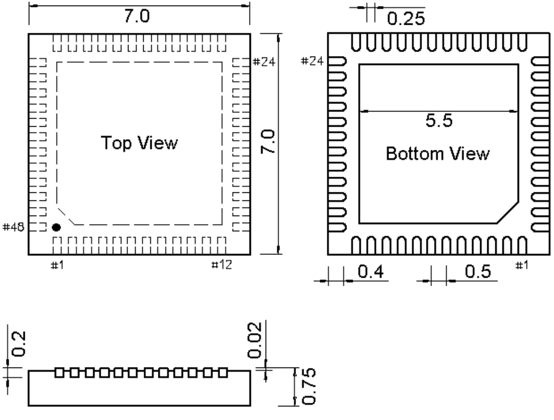
2. Bản vẽ Kích thước Vỏ (D×E×A)PACKAGE DIMENSIONS
CH32V103R8T6 - 2. Bản vẽ Kích thước Vỏ (D×E×A)
LQFP-64M(10x10) · 10.00×10.00mm · Pitch 0.50mmPhóng to ›
3. Bản vẽ Footprint Khuyến nghịLAND PATTERN
CH32V103R8T6 - 3. Bản vẽ Footprint Khuyến nghị
IPC-7351B Land Pattern (64 Pads)Phóng to ›
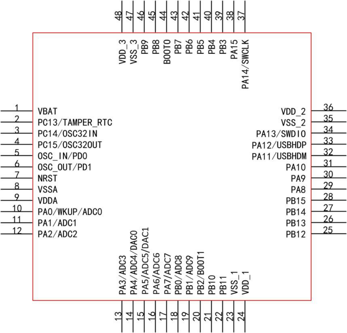
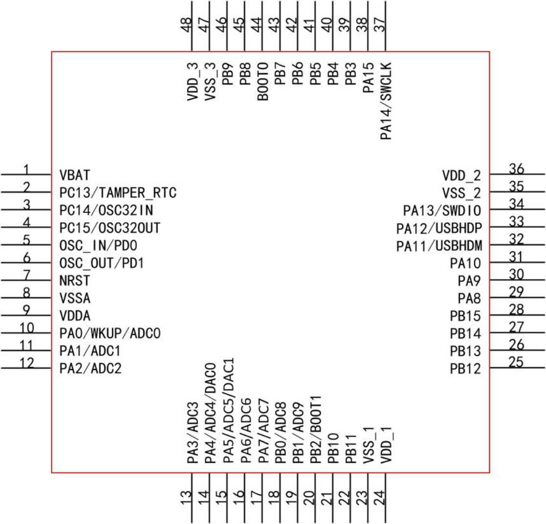
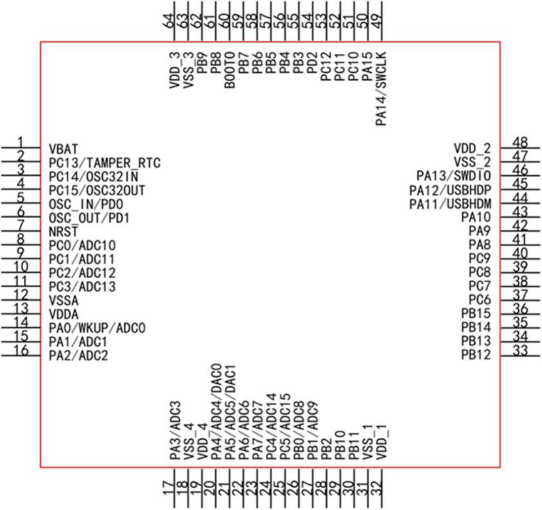
4. Sơ đồ Chân Gốc PDF (Pinout)PINOUT DIAGRAM
CH32V103R8T6 - 4. Sơ đồ Chân Gốc PDF (Pinout)
Cấu hình 64 chân từ DatasheetPhóng to ›
5. Mạch Nguyên lý Ứng dụngSCHEMATIC
CH32V103R8T6 - 5. Mạch Nguyên lý Ứng dụng
Typical Application SchematicPhóng to ›
Hình ảnh & Biểu đồ Cắt tự động từ PDF Datasheet (12 hình · Trang 1/1)
Hiển thị hình 1–12 trên tổng 12 hình đúng phiên bản CH32V103R8T6
Trang 1 · p01_fig01279×170px
CH32V103R8T6 p01_fig01
Overview
Trang 13 · p13_fig011095×1030px
CH32V103R8T6 p13_fig01
CH32V103Cx
Trang 13 · p13_fig021117×1072px
CH32V103R8T6 p13_fig02
V1.2 11
Trang 13 · p13_fig02Trang 13
CH32V103R8T6 p13_fig02
Datasheet Page 13 (p13_fig02)
Trang 16 · p16_fig012009×2623px
CH32V103R8T6 p16_fig01
V1.2 14
Trang 36 · p36_fig011191×329px
CH32V103R8T6 p36_fig01
CH32V103 Datasheet https://wch-ic.com
Trang 36 · p36_fig021284×434px
CH32V103R8T6 p36_fig02
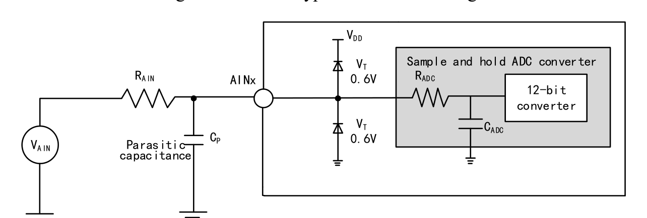
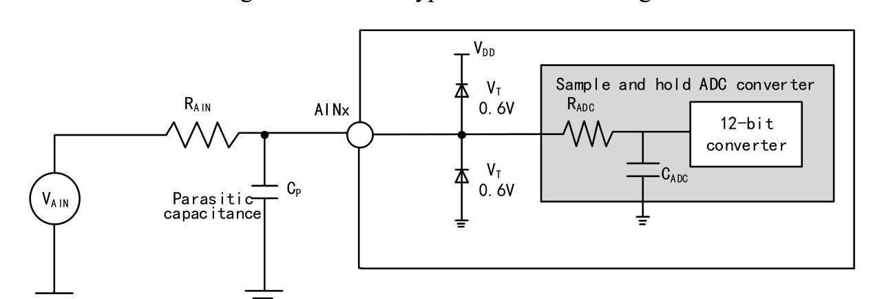
Figure 3-12 ADC typical connection diagram
Trang 36 · p36_fig01Trang 36
CH32V103R8T6 p36_fig01
Datasheet Page 36 (p36_fig01)
Trang 36 · p36_fig02Trang 36
CH32V103R8T6 p36_fig02
Datasheet Page 36 (p36_fig02)
Trang 39 · p39_fig011095×832px
CH32V103R8T6 p39_fig01
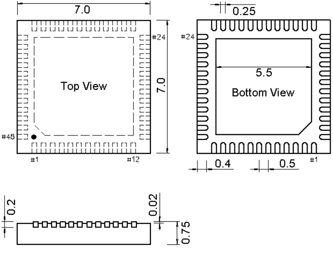
Figure 4-3 QFN48×7 package
Trang 39 · p39_fig01Trang 39
CH32V103R8T6 p39_fig01
Datasheet Page 39 (p39_fig01)
Trang 40 · p40_fig011510×1666px
CH32V103R8T6 p40_fig01
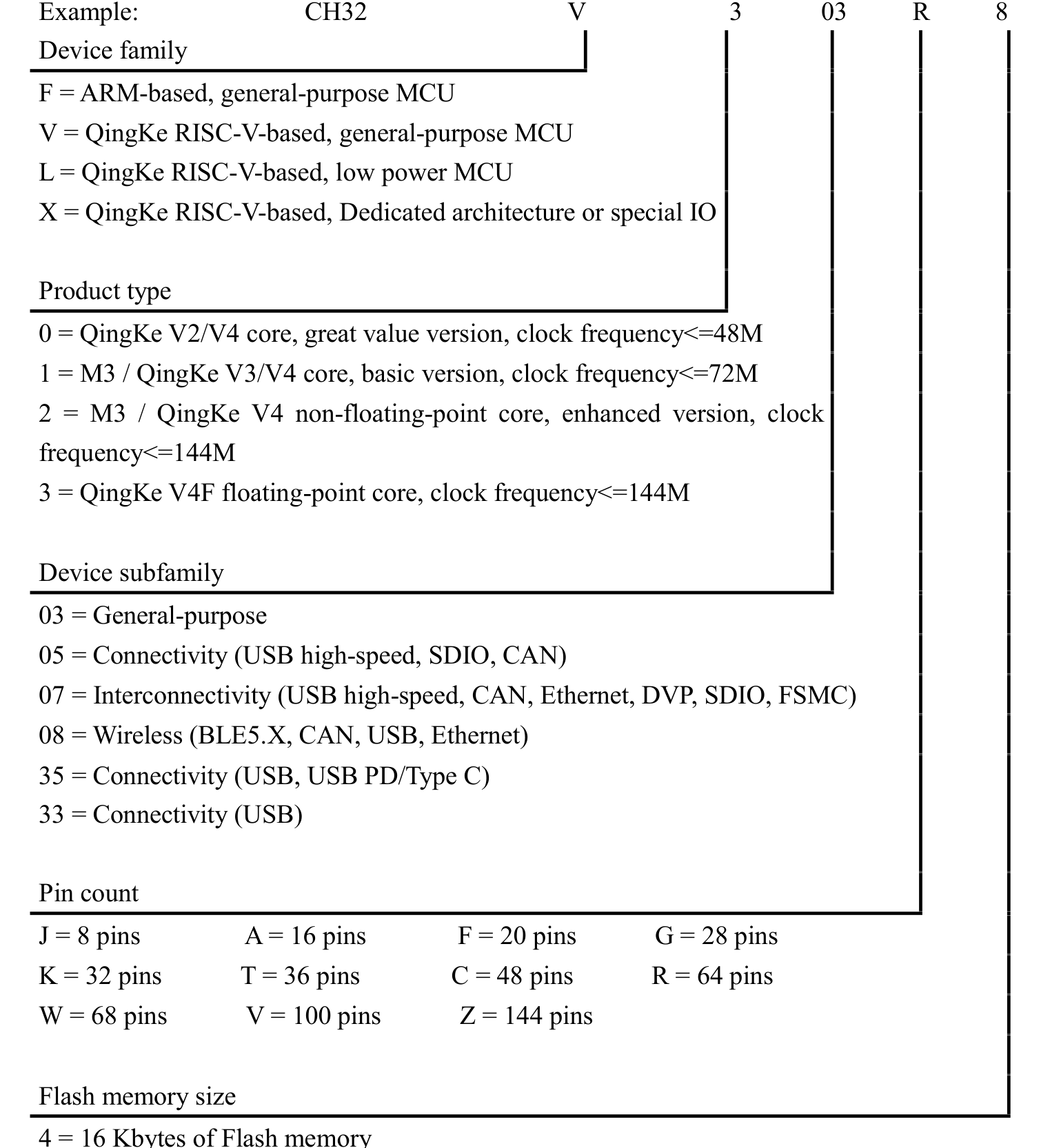
7 = 48 Kbytes of Flash memory

Thông số Kỹ thuật Trích xuất từ Datasheet (EN)

CH32V103R8T6 (LQFP-64M(10x10)) is a 64-pin embedded microcontroller unit (mcu) featuring a 10.00 × 10.00 × 1.40 mm mechanical envelope (lead pitch e = 0.50 mm). Rated for 2.7V~5.5V supply operation across -40°C ~ +85°C (Industrial Grade) with integrated USB, UART, SPI, I2C, ADC, PWM, IrDA, RTC/CLK interfaces.
Embedded Microcontroller Unit (MCU)
Operating Supply VoltageV_CC / V_DD
2.7V~5.5V
Place 100nF + 10µF X7R decoupling capacitors < 2mm from supply pins
Ambient Operating TemperatureT_A
-40°C ~ +85°C (Industrial Grade)
Industrial temperature grade; T_J(max) = +125°C
Clock / RF Operating Frequencyf_CLK / f_RF
80MHz
Extracted from authoritative PDF specification tables
Current & Power RatingI_OUT / I_CC
I_GPIO(max) = ±20 mA / pin | I_VDD(total) ≤ 150 mA
Observe per-pin absolute maximum current limits
Package Envelope (D × E × A)D × E × A
10.00 × 10.00 × 1.40 mm (A1=0.10 mm)
Package family: LQFP (LQFP-64M(10x10))
Pin Count & Lead PitchN / e
64 Pins | Pitch e = 0.50 mm (19.7 mil)
Normalized to Center-to-Center Span C per IPC-7351B
Integrated Peripheral InterfacesBuses
USB, UART, SPI, I2C, ADC, PWM, IrDA, RTC/CLK
Cross-linked with 4D Pinout & Schematic Symbol
Reflow & Moisture SensitivityIPC / MSL
IPC-7351B Level B | J-STD-020 (Peak 260°C) | MSL-3
60% windowed solder paste stencil on thermal EPAD
Cảnh báo: Boot Strapping Pin Alert (BOOT0): Do not force conflicting external pull-ups/pull-downs during POR reset.
Cảnh báo: Connect exposed thermal pad (if present) to internal ground plane via 0.3mm stitched thermal vias.

Kiểm định 5 Chuẩn

Đánh giá tự động trước khi xuất file
5/5 PASS
✓
IEEE-315 Symbol64 chân phân nhóm tự động
OK
✓
IPC-7351B Land Pattern64 pads · Pitch 0.50mm
OK
✓
IPC-7525 Kem hàn 60%Chuẩn Reflow 1:1
OK
✓
DFM JLCPCB / PCBWayKhe hở Pad min: 0.25mm
OK
✓
3D STEP AP214 & GLBKhớp gốc tọa độ (0,0,0)
OK

Xác nhận Mạch Thật & Đánh giá Kỹ thuật

Chia sẻ kết quả đặt mạch thực tế (JLCPCB / PCBWay) hoặc gửi góp ý cải thiện thư viện
★ 5.00 PCB Verified

Kích thước Cơ khí & Land Pattern (LQFP-64M(10x10))

Trích xuất từ Datasheet & chuẩn hóa IPC-7351B
mm
Thân vỏ (D × E)Nominal
10.00 × 10.00 mm
Chiều cao (A) & Pitch (e)IPC-7351B
A=1.40mm · e=0.50mm
Kích thước Pad (W × L)Level B
0.30 × 1.25 mm
Số chân / Tổng số PadTopology
64P / 64Pad (QUAD_ROW)

BOM Ngoại vi Khuyến nghị & Mã IC Tương đương (Drop-in)

Linh kiện thụ động đi kèm theo sơ đồ nguyên lý tiêu chuẩn và các mã thay thế tương thích chân 1:1
DFM READY
Ký hiệu / Mã thay thếGiá trị / Kiểu vỏVai trò & Quy tắc Bố trí PCB (Layout Rule)
C1
Passive
100nF X7R
0402 / 0603
Đảm bảo bề rộng đường mạch phù hợp dòng định mức

Câu hỏi Kỹ thuật Thường gặp (FAQ) — CH32V103R8T6 (LQFP-64M(10x10))

Giải đáp nhanh về sơ đồ chân Pinout, kích thước Land Pattern IPC-7351B và định dạng tệp CAD
IPC-7351B / IEEE-315

Sơ đồ chân (Pinout) và thông số điện áp của CH32V103R8T6 (LQFP-64M(10x10)) như thế nào?

Linh kiện CH32V103R8T6 do WCH sản xuất đóng gói kiểu LQFP-64M(10x10) gồm 64 chân với bước chân (pitch) 0.50 mm, dải điện áp hoạt động VCC 2.7V~5.5V. Các chân tiêu biểu gồm: Chân 1 (VBAT: Chân cấp nguồn dương (VBAT — 2.7V~5.5V)), Chân 2 (PC13-TAMPER-RTC: Chân Đa năng Vào/Ra & Ngoại vi PC13-TAMPER-RTC (RTC/CLK)), Chân 3 (PC14-OSC32_IN: Chân Đa năng Vào/Ra & Ngoại vi PC14-OSC32_IN (RTC/CLK)), Chân 4 (PC15-OSC32_OUT: Chân Đa năng Vào/Ra & Ngoại vi PC15-OSC32_OUT (RTC/CLK)), Chân 5 (OSC_IN: Chân Đa năng Vào/Ra & Ngoại vi OSC_IN (RTC/CLK)), Chân 6 (OSC_OUT: Chân Đa năng Vào/Ra & Ngoại vi OSC_OUT (RTC/CLK)).

Kích thước Footprint chuẩn IPC-7351B của CH32V103R8T6 là bao nhiêu?

Theo bản vẽ cơ khí Datasheet và chuẩn hóa toán học IPC-7351B (Density Level B Nominal), thân vỏ CH32V103R8T6 (LQFP-64M(10x10)) có kích thước danh định 10.00 × 10.00 mm, bước chân e = 0.50 mm, tổng số 64 pad đồng.

Tải thư viện KiCad (.kicad_mod, .kicad_sym), Fusion 360 (.lbr) và mô hình 3D STEP cho CH32V103R8T6 ở đâu?

Bạn có thể tải trực tiếp và miễn phí (giấy phép mở CERN-OHL-P-2.0) toàn bộ gói thư viện CAD đã hậu kiểm của CH32V103R8T6 (WCH, LQFP-64M(10x10)) ngay trên trang này, bao gồm: KiCad 8 Footprint (.kicad_mod), KiCad Schematic Symbol (.kicad_sym), Autodesk Fusion 360 / Eagle (.lbr), và mô hình 3D MCAD (.STEP AP214 & WebGL .GLB).