
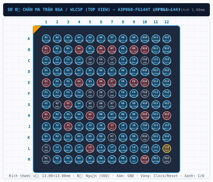
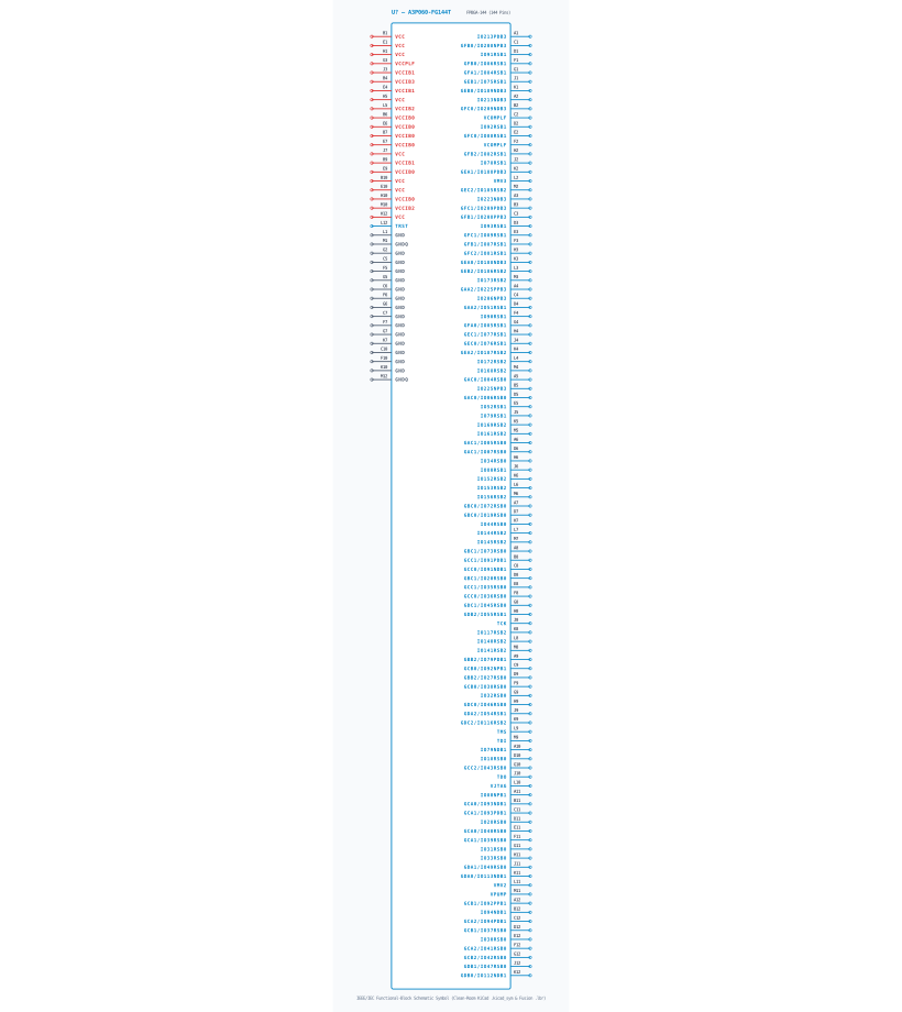
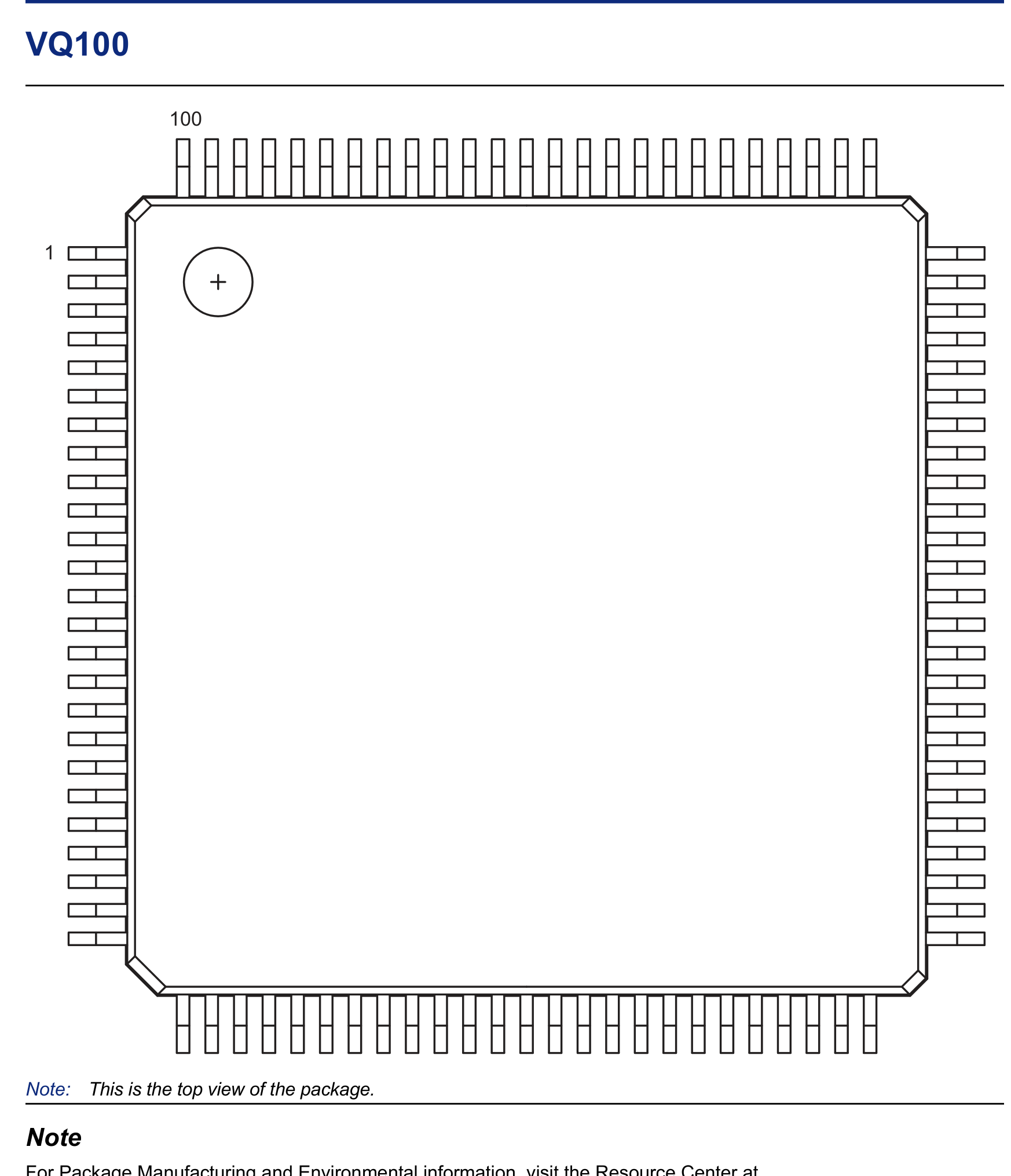
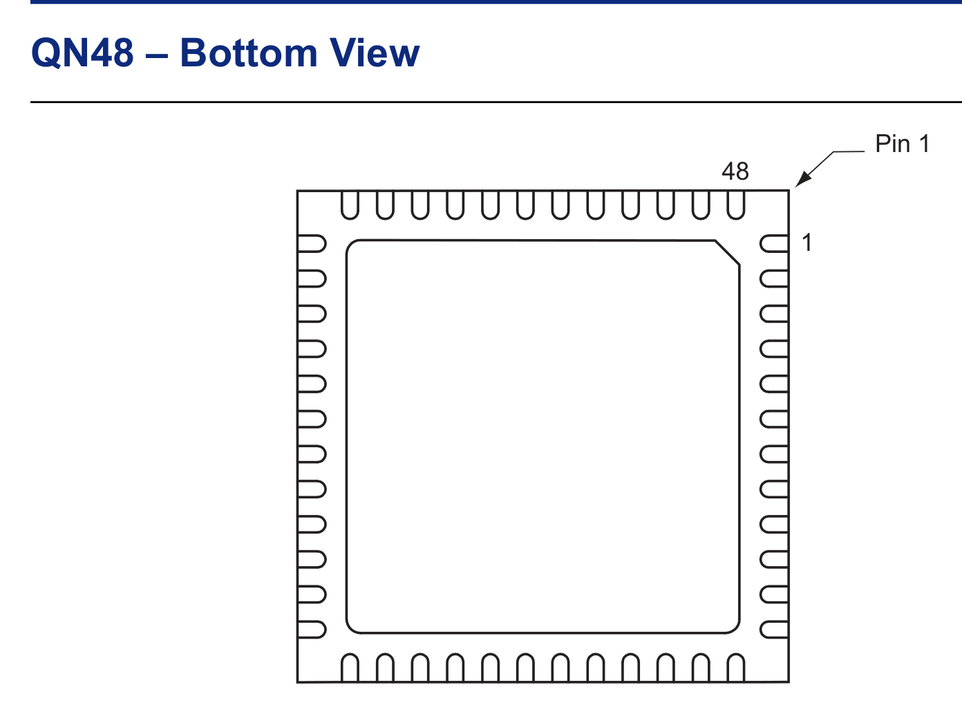
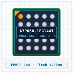
FPBGA-144 · 144P
IPC-7351B
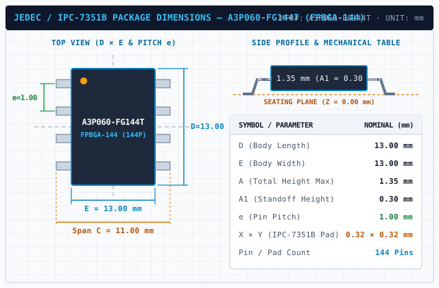
144P13.0×13.0×1.35mmP=1mm
A3P060 / A3P125 / A3P400 (FPBGA-144)
| Pin | Symbol | Typ | Funktionsbeschreibung (DE) |
|---|---|---|---|
| A1 | IO213PDB3 | I/O | Multiplex-I/O- & Peripherie-Pin IO213PDB3 (General) |
| A2 | IO213NDB3 | I/O | Multiplex-I/O- & Peripherie-Pin IO213NDB3 (General) |
| A3 | IO223NDB3 | I/O | Multiplex-I/O- & Peripherie-Pin IO223NDB3 (General) |
| A4 | GAA2/IO225PPB3 | I/O | Multiplex-I/O- & Peripherie-Pin GAA2/IO225PPB3 (General) |
| A5 | GAC0/IO04RSB0 | I/O | Multiplex-I/O- & Peripherie-Pin GAC0/IO04RSB0 (General) |
| A6 | GAC1/IO05RSB0 | I/O | Multiplex-I/O- & Peripherie-Pin GAC1/IO05RSB0 (General) |
| A7 | GBC0/IO72RSB0 | I/O | Multiplex-I/O- & Peripherie-Pin GBC0/IO72RSB0 (General) |
| A8 | GBC1/IO73RSB0 | I/O | Multiplex-I/O- & Peripherie-Pin GBC1/IO73RSB0 (General) |
| A9 | GBB2/IO79PDB1 | I/O | Multiplex-I/O- & Peripherie-Pin GBB2/IO79PDB1 (General) |
| A10 | IO79NDB1 | I/O | Multiplex-I/O- & Peripherie-Pin IO79NDB1 (General) |
| A11 | IO80NPB1 | I/O | Multiplex-I/O- & Peripherie-Pin IO80NPB1 (General) |
| A12 | GCB1/IO92PPB1 | I/O | Multiplex-I/O- & Peripherie-Pin GCB1/IO92PPB1 (General) |
| B1 | VCC | Power | Versorgungsspannungseingang (VCC — 3 V to 3.6 V) |
| B2 | GFC0/IO209NDB3 | I/O | Multiplex-I/O- & Peripherie-Pin GFC0/IO209NDB3 (General) |
| B3 | GFC1/IO209PDB3 | I/O | Multiplex-I/O- & Peripherie-Pin GFC1/IO209PDB3 (General) |
| B4 | VCCIB3 | Power | Versorgungsspannungseingang (VCCIB3 — 3 V to 3.6 V) |
| B5 | IO225NPB3 | I/O | Multiplex-I/O- & Peripherie-Pin IO225NPB3 (General) |
| B6 | VCCIB0 | Power | Versorgungsspannungseingang (VCCIB0 — 3 V to 3.6 V) |
| B7 | VCCIB0 | Power | Versorgungsspannungseingang (VCCIB0 — 3 V to 3.6 V) |
| B8 | GCC1/IO91PDB1 | I/O | Multiplex-I/O- & Peripherie-Pin GCC1/IO91PDB1 (General) |
| B9 | VCCIB1 | Power | Versorgungsspannungseingang (VCCIB1 — 3 V to 3.6 V) |
| B10 | VCC | Power | Versorgungsspannungseingang (VCC — 3 V to 3.6 V) |
| B11 | GCA0/IO93NDB1 | I/O | Multiplex-I/O- & Peripherie-Pin GCA0/IO93NDB1 (General) |
| B12 | IO94NDB1 | I/O | Multiplex-I/O- & Peripherie-Pin IO94NDB1 (General) |
| C1 | GFB0/IO208NPB3 | I/O | Multiplex-I/O- & Peripherie-Pin GFB0/IO208NPB3 (General) |
| C2 | VCOMPLF | I/O | Multiplex-I/O- & Peripherie-Pin VCOMPLF (General) |
| C3 | GFB1/IO208PPB3 | I/O | Multiplex-I/O- & Peripherie-Pin GFB1/IO208PPB3 (General) |
| C4 | IO206NPB3 | I/O | Multiplex-I/O- & Peripherie-Pin IO206NPB3 (General) |
| C5 | GND | GND | Masseanschluss (GND) |
| C6 | GND | GND | Masseanschluss (GND) |
| C7 | GND | GND | Masseanschluss (GND) |
| C8 | GCC0/IO91NDB1 | I/O | Multiplex-I/O- & Peripherie-Pin GCC0/IO91NDB1 (General) |
| C9 | GCB0/IO92NPB1 | I/O | Multiplex-I/O- & Peripherie-Pin GCB0/IO92NPB1 (General) |
| C10 | GND | GND | Masseanschluss (GND) |
| C11 | GCA1/IO93PDB1 | I/O | Multiplex-I/O- & Peripherie-Pin GCA1/IO93PDB1 (General) |
| C12 | GCA2/IO94PDB1 | I/O | Multiplex-I/O- & Peripherie-Pin GCA2/IO94PDB1 (General) |
| D1 | IO91RSB1 | I/O | Multiplex-I/O- & Peripherie-Pin IO91RSB1 (General) |
| D2 | IO92RSB1 | I/O | Multiplex-I/O- & Peripherie-Pin IO92RSB1 (General) |
| D3 | IO93RSB1 | I/O | Multiplex-I/O- & Peripherie-Pin IO93RSB1 (General) |
| D4 | GAA2/IO51RSB1 | I/O | Multiplex-I/O- & Peripherie-Pin GAA2/IO51RSB1 (General) |
| D5 | GAC0/IO06RSB0 | I/O | Multiplex-I/O- & Peripherie-Pin GAC0/IO06RSB0 (General) |
| D6 | GAC1/IO07RSB0 | I/O | Multiplex-I/O- & Peripherie-Pin GAC1/IO07RSB0 (General) |
| D7 | GBC0/IO19RSB0 | I/O | Multiplex-I/O- & Peripherie-Pin GBC0/IO19RSB0 (General) |
| D8 | GBC1/IO20RSB0 | I/O | Multiplex-I/O- & Peripherie-Pin GBC1/IO20RSB0 (General) |
| D9 | GBB2/IO27RSB0 | I/O | Multiplex-I/O- & Peripherie-Pin GBB2/IO27RSB0 (General) |
| D10 | IO18RSB0 | I/O | Multiplex-I/O- & Peripherie-Pin IO18RSB0 (General) |
| D11 | IO28RSB0 | I/O | Multiplex-I/O- & Peripherie-Pin IO28RSB0 (General) |
| D12 | GCB1/IO37RSB0 | I/O | Multiplex-I/O- & Peripherie-Pin GCB1/IO37RSB0 (General) |
| E1 | VCC | Power | Versorgungsspannungseingang (VCC — 3 V to 3.6 V) |
| E2 | GFC0/IO88RSB1 | I/O | Multiplex-I/O- & Peripherie-Pin GFC0/IO88RSB1 (General) |
| E3 | GFC1/IO89RSB1 | I/O | Multiplex-I/O- & Peripherie-Pin GFC1/IO89RSB1 (General) |
| E4 | VCCIB1 | Power | Versorgungsspannungseingang (VCCIB1 — 3 V to 3.6 V) |
| E5 | IO52RSB1 | I/O | Multiplex-I/O- & Peripherie-Pin IO52RSB1 (General) |
| E6 | VCCIB0 | Power | Versorgungsspannungseingang (VCCIB0 — 3 V to 3.6 V) |
| E7 | VCCIB0 | Power | Versorgungsspannungseingang (VCCIB0 — 3 V to 3.6 V) |
| E8 | GCC1/IO35RSB0 | I/O | Multiplex-I/O- & Peripherie-Pin GCC1/IO35RSB0 (General) |
| E9 | VCCIB0 | Power | Versorgungsspannungseingang (VCCIB0 — 3 V to 3.6 V) |
| E10 | VCC | Power | Versorgungsspannungseingang (VCC — 3 V to 3.6 V) |
| E11 | GCA0/IO40RSB0 | I/O | Multiplex-I/O- & Peripherie-Pin GCA0/IO40RSB0 (General) |
| E12 | IO30RSB0 | I/O | Multiplex-I/O- & Peripherie-Pin IO30RSB0 (General) |
| F1 | GFB0/IO86RSB1 | I/O | Multiplex-I/O- & Peripherie-Pin GFB0/IO86RSB1 (General) |
| F2 | VCOMPLF | I/O | Multiplex-I/O- & Peripherie-Pin VCOMPLF (General) |
| F3 | GFB1/IO87RSB1 | I/O | Multiplex-I/O- & Peripherie-Pin GFB1/IO87RSB1 (General) |
| F4 | IO90RSB1 | I/O | Multiplex-I/O- & Peripherie-Pin IO90RSB1 (General) |
| F5 | GND | GND | Masseanschluss (GND) |
| F6 | GND | GND | Masseanschluss (GND) |
| F7 | GND | GND | Masseanschluss (GND) |
| F8 | GCC0/IO36RSB0 | I/O | Multiplex-I/O- & Peripherie-Pin GCC0/IO36RSB0 (General) |
| F9 | GCB0/IO38RSB0 | I/O | Multiplex-I/O- & Peripherie-Pin GCB0/IO38RSB0 (General) |
| F10 | GND | GND | Masseanschluss (GND) |
| F11 | GCA1/IO39RSB0 | I/O | Multiplex-I/O- & Peripherie-Pin GCA1/IO39RSB0 (General) |
| F12 | GCA2/IO41RSB0 | I/O | Multiplex-I/O- & Peripherie-Pin GCA2/IO41RSB0 (General) |
| G1 | GFA1/IO84RSB1 | I/O | Multiplex-I/O- & Peripherie-Pin GFA1/IO84RSB1 (General) |
| G2 | GND | GND | Masseanschluss (GND) |
| G3 | VCCPLF | Power | Versorgungsspannungseingang (VCCPLF — 3 V to 3.6 V) |
| G4 | GFA0/IO85RSB1 | I/O | Multiplex-I/O- & Peripherie-Pin GFA0/IO85RSB1 (General) |
| G5 | GND | GND | Masseanschluss (GND) |
| G6 | GND | GND | Masseanschluss (GND) |
| G7 | GND | GND | Masseanschluss (GND) |
| G8 | GDC1/IO45RSB0 | I/O | Multiplex-I/O- & Peripherie-Pin GDC1/IO45RSB0 (General) |
| G9 | IO32RSB0 | I/O | Multiplex-I/O- & Peripherie-Pin IO32RSB0 (General) |
| G10 | GCC2/IO43RSB0 | I/O | Multiplex-I/O- & Peripherie-Pin GCC2/IO43RSB0 (General) |
| G11 | IO31RSB0 | I/O | Multiplex-I/O- & Peripherie-Pin IO31RSB0 (General) |
| G12 | GCB2/IO42RSB0 | I/O | Multiplex-I/O- & Peripherie-Pin GCB2/IO42RSB0 (General) |
| H1 | VCC | Power | Versorgungsspannungseingang (VCC — 3 V to 3.6 V) |
| H2 | GFB2/IO82RSB1 | I/O | Multiplex-I/O- & Peripherie-Pin GFB2/IO82RSB1 (General) |
| H3 | GFC2/IO81RSB1 | I/O | Multiplex-I/O- & Peripherie-Pin GFC2/IO81RSB1 (General) |
| H4 | GEC1/IO77RSB1 | I/O | Multiplex-I/O- & Peripherie-Pin GEC1/IO77RSB1 (General) |
| H5 | VCC | Power | Versorgungsspannungseingang (VCC — 3 V to 3.6 V) |
| H6 | IO34RSB0 | I/O | Multiplex-I/O- & Peripherie-Pin IO34RSB0 (General) |
| H7 | IO44RSB0 | I/O | Multiplex-I/O- & Peripherie-Pin IO44RSB0 (General) |
| H8 | GDB2/IO55RSB1 | I/O | Multiplex-I/O- & Peripherie-Pin GDB2/IO55RSB1 (General) |
| H9 | GDC0/IO46RSB0 | I/O | Multiplex-I/O- & Peripherie-Pin GDC0/IO46RSB0 (General) |
| H10 | VCCIB0 | Power | Versorgungsspannungseingang (VCCIB0 — 3 V to 3.6 V) |
| H11 | IO33RSB0 | I/O | Multiplex-I/O- & Peripherie-Pin IO33RSB0 (General) |
| H12 | VCC | Power | Versorgungsspannungseingang (VCC — 3 V to 3.6 V) |
| J1 | GEB1/IO75RSB1 | I/O | Multiplex-I/O- & Peripherie-Pin GEB1/IO75RSB1 (General) |
| J2 | IO78RSB1 | I/O | Multiplex-I/O- & Peripherie-Pin IO78RSB1 (General) |
| J3 | VCCIB1 | Power | Versorgungsspannungseingang (VCCIB1 — 3 V to 3.6 V) |
| J4 | GEC0/IO76RSB1 | I/O | Multiplex-I/O- & Peripherie-Pin GEC0/IO76RSB1 (General) |
| J5 | IO79RSB1 | I/O | Multiplex-I/O- & Peripherie-Pin IO79RSB1 (General) |
| J6 | IO80RSB1 | I/O | Multiplex-I/O- & Peripherie-Pin IO80RSB1 (General) |
| J7 | VCC | Power | Versorgungsspannungseingang (VCC — 3 V to 3.6 V) |
| J8 | TCK | I/O | Multiplex-I/O- & Peripherie-Pin TCK (General) |
| J9 | GDA2/IO54RSB1 | I/O | Multiplex-I/O- & Peripherie-Pin GDA2/IO54RSB1 (General) |
| J10 | TDO | I/O | Multiplex-I/O- & Peripherie-Pin TDO (General) |
| J11 | GDA1/IO49RSB0 | I/O | Multiplex-I/O- & Peripherie-Pin GDA1/IO49RSB0 (General) |
| J12 | GDB1/IO47RSB0 | I/O | Multiplex-I/O- & Peripherie-Pin GDB1/IO47RSB0 (General) |
| K1 | GEB0/IO189NDB3 | I/O | Multiplex-I/O- & Peripherie-Pin GEB0/IO189NDB3 (General) |
| K2 | GEA1/IO188PDB3 | I/O | Multiplex-I/O- & Peripherie-Pin GEA1/IO188PDB3 (General) |
| K3 | GEA0/IO188NDB3 | I/O | Multiplex-I/O- & Peripherie-Pin GEA0/IO188NDB3 (General) |
| K4 | GEA2/IO187RSB2 | I/O | Multiplex-I/O- & Peripherie-Pin GEA2/IO187RSB2 (General) |
| K5 | IO169RSB2 | I/O | Multiplex-I/O- & Peripherie-Pin IO169RSB2 (General) |
| K6 | IO152RSB2 | I/O | Multiplex-I/O- & Peripherie-Pin IO152RSB2 (General) |
| K7 | GND | GND | Masseanschluss (GND) |
| K8 | IO117RSB2 | I/O | Multiplex-I/O- & Peripherie-Pin IO117RSB2 (General) |
| K9 | GDC2/IO116RSB2 | I/O | Multiplex-I/O- & Peripherie-Pin GDC2/IO116RSB2 (General) |
| K10 | GND | GND | Masseanschluss (GND) |
| K11 | GDA0/IO113NDB1 | I/O | Multiplex-I/O- & Peripherie-Pin GDA0/IO113NDB1 (General) |
| K12 | GDB0/IO112NDB1 | I/O | Multiplex-I/O- & Peripherie-Pin GDB0/IO112NDB1 (General) |
| L1 | GND | GND | Masseanschluss (GND) |
| L2 | VMV3 | I/O | Multiplex-I/O- & Peripherie-Pin VMV3 (General) |
| L3 | GEB2/IO186RSB2 | I/O | Multiplex-I/O- & Peripherie-Pin GEB2/IO186RSB2 (General) |
| L4 | IO172RSB2 | I/O | Multiplex-I/O- & Peripherie-Pin IO172RSB2 (General) |
| L5 | VCCIB2 | Power | Versorgungsspannungseingang (VCCIB2 — 3 V to 3.6 V) |
| L6 | IO153RSB2 | I/O | Multiplex-I/O- & Peripherie-Pin IO153RSB2 (General) |
| L7 | IO144RSB2 | I/O | Multiplex-I/O- & Peripherie-Pin IO144RSB2 (General) |
| L8 | IO140RSB2 | I/O | Multiplex-I/O- & Peripherie-Pin IO140RSB2 (General) |
| L9 | TMS | I/O | Multiplex-I/O- & Peripherie-Pin TMS (General) |
| L10 | VJTAG | I/O | Multiplex-I/O- & Peripherie-Pin VJTAG (General) |
| L11 | VMV2 | I/O | Multiplex-I/O- & Peripherie-Pin VMV2 (General) |
| L12 | TRST | I/O | Multiplex-I/O- & Peripherie-Pin TRST (General) |
| M1 | GNDQ | GND | Masseanschluss (GNDQ) |
| M2 | GEC2/IO185RSB2 | I/O | Multiplex-I/O- & Peripherie-Pin GEC2/IO185RSB2 (General) |
| M3 | IO173RSB2 | I/O | Multiplex-I/O- & Peripherie-Pin IO173RSB2 (General) |
| M4 | IO168RSB2 | I/O | Multiplex-I/O- & Peripherie-Pin IO168RSB2 (General) |
| M5 | IO161RSB2 | I/O | Multiplex-I/O- & Peripherie-Pin IO161RSB2 (General) |
| M6 | IO156RSB2 | I/O | Multiplex-I/O- & Peripherie-Pin IO156RSB2 (General) |
| M7 | IO145RSB2 | I/O | Multiplex-I/O- & Peripherie-Pin IO145RSB2 (General) |
| M8 | IO141RSB2 | I/O | Multiplex-I/O- & Peripherie-Pin IO141RSB2 (General) |
| M9 | TDI | I/O | Multiplex-I/O- & Peripherie-Pin TDI (General) |
| M10 | VCCIB2 | Power | Versorgungsspannungseingang (VCCIB2 — 3 V to 3.6 V) |
| M11 | VPUMP | I/O | Multiplex-I/O- & Peripherie-Pin VPUMP (General) |
| M12 | GNDQ | GND | Masseanschluss (GNDQ) |
A3P060 / A3P125 / A3P400 (FPBGA-144)
A3P060 / A3P125 / A3P400 (FPBGA-144)
A3P060 / A3P125 / A3P400 (FPBGA-144)
A3P060 / A3P125 / A3P400 (FPBGA-144)
A3P060 / A3P125 / A3P400 (FPBGA-144)
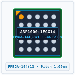
A3P060 / A3P125 / A3P400 (FPBGA-144(13x13))
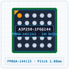
A3P060 / A3P125 / A3P400 (FPBGA-144(13x13))
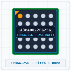
A3P060 / A3P125 / A3P400 (FPBGA-256)
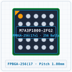
A3P060 / A3P125 / A3P400 (FPBGA-256(17x17))
A3P060 / A3P125 / A3P400 (FPBGA-484)
A3P060 / A3P125 / A3P400 (FPBGA-484)
A3P060 / A3P125 / A3P400 (FPBGA-484)
| Bauteilbezeichner / Ersatz-MPN | Wert / Gehäuse | Funktion & PCB-Layout-Regel |
|---|---|---|
| N/A BOM | Per application circuit FPBGA-144 | Leiterbahnbreiten für Nennstrom dimensionieren und IPC-2221 Isolationsabstände einhalten. |
Das Bauteil A3P060-FG144T von MICROCHIP im FPBGA-144-Gehäuse besitzt 144 Pins mit einem Rastermaß (Pitch) von 1.00 mm und einem Betriebsspannungsbereich VCC von 3 V to 3.6 V. Wichtige Pins: A1 (IO213PDB3: Multiplex-I/O- & Peripherie-Pin IO213PDB3 (General)), A2 (IO213NDB3: Multiplex-I/O- & Peripherie-Pin IO213NDB3 (General)), A3 (IO223NDB3: Multiplex-I/O- & Peripherie-Pin IO223NDB3 (General)), A4 (GAA2/IO225PPB3: Multiplex-I/O- & Peripherie-Pin GAA2/IO225PPB3 (General)), A5 (GAC0/IO04RSB0: Multiplex-I/O- & Peripherie-Pin GAC0/IO04RSB0 (General)), A6 (GAC1/IO05RSB0: Multiplex-I/O- & Peripherie-Pin GAC1/IO05RSB0 (General)).
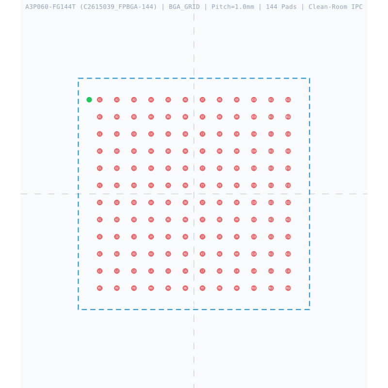
Gemäß Datenblatt und IPC-7351B (Density Level B Nominal) betragen die Gehäusemaße des A3P060-FG144T (FPBGA-144) 13.00 × 13.00 mm bei einem Pitch e = 1.00 mm und 144 Kupfer-Pads.
Auf dieser Seite können Sie das vollständig verifizierte CAD-Bibliothekspaket für A3P060-FG144T (MICROCHIP, FPBGA-144) unter der Open-Hardware-Lizenz CERN-OHL-P-2.0 kostenlos herunterladen: KiCad 8 Footprint (.kicad_mod), Schaltplansymbol (.kicad_sym), Fusion 360 / Eagle (.lbr) und 3D STEP AP214 / WebGL GLB.
| Pin-Nr. | Signalname | Elektrischer Typ | Funktionsbeschreibung & Schaltungshinweise |
|---|---|---|---|
| A1 | IO213PDB3 | Digital_IO | Signalanschluss IO213PDB3 (Richtung: I/O, Spannungsbereich: 3 V to 3.6 V). Alternative Multiplex-Funktionen: IO213PDB3. Unterstützte Bus-Schnittstellen: General. |
| A2 | IO213NDB3 | Digital_IO | Signalanschluss IO213NDB3 (Richtung: I/O, Spannungsbereich: 3 V to 3.6 V). Alternative Multiplex-Funktionen: IO213NDB3. Unterstützte Bus-Schnittstellen: General. |
| A3 | IO223NDB3 | Digital_IO | Signalanschluss IO223NDB3 (Richtung: I/O, Spannungsbereich: 3 V to 3.6 V). Alternative Multiplex-Funktionen: IO223NDB3. Unterstützte Bus-Schnittstellen: General. |
| A4 | GAA2/IO225PPB3 | Digital_IO | Signalanschluss GAA2/IO225PPB3 (Richtung: I/O, Spannungsbereich: 3 V to 3.6 V). Alternative Multiplex-Funktionen: GAA2/IO225PPB3. Unterstützte Bus-Schnittstellen: General. |
| A5 | GAC0/IO04RSB0 | Digital_IO | Signalanschluss GAC0/IO04RSB0 (Richtung: I/O, Spannungsbereich: 3 V to 3.6 V). Alternative Multiplex-Funktionen: GAC0/IO04RSB0. Unterstützte Bus-Schnittstellen: General. |
| A6 | GAC1/IO05RSB0 | Digital_IO | Signalanschluss GAC1/IO05RSB0 (Richtung: I/O, Spannungsbereich: 3 V to 3.6 V). Alternative Multiplex-Funktionen: GAC1/IO05RSB0. Unterstützte Bus-Schnittstellen: General. |
| A7 | GBC0/IO72RSB0 | Digital_IO | Signalanschluss GBC0/IO72RSB0 (Richtung: I/O, Spannungsbereich: 3 V to 3.6 V). Alternative Multiplex-Funktionen: GBC0/IO72RSB0. Unterstützte Bus-Schnittstellen: General. |
| A8 | GBC1/IO73RSB0 | Digital_IO | Signalanschluss GBC1/IO73RSB0 (Richtung: I/O, Spannungsbereich: 3 V to 3.6 V). Alternative Multiplex-Funktionen: GBC1/IO73RSB0. Unterstützte Bus-Schnittstellen: General. |
| A9 | GBB2/IO79PDB1 | Digital_IO | Signalanschluss GBB2/IO79PDB1 (Richtung: I/O, Spannungsbereich: 3 V to 3.6 V). Alternative Multiplex-Funktionen: GBB2/IO79PDB1. Unterstützte Bus-Schnittstellen: General. |
| A10 | IO79NDB1 | Digital_IO | Signalanschluss IO79NDB1 (Richtung: I/O, Spannungsbereich: 3 V to 3.6 V). Alternative Multiplex-Funktionen: IO79NDB1. Unterstützte Bus-Schnittstellen: General. |
| A11 | IO80NPB1 | Digital_IO | Signalanschluss IO80NPB1 (Richtung: I/O, Spannungsbereich: 3 V to 3.6 V). Alternative Multiplex-Funktionen: IO80NPB1. Unterstützte Bus-Schnittstellen: General. |
| A12 | GCB1/IO92PPB1 | Digital_IO | Signalanschluss GCB1/IO92PPB1 (Richtung: I/O, Spannungsbereich: 3 V to 3.6 V). Alternative Multiplex-Funktionen: GCB1/IO92PPB1. Unterstützte Bus-Schnittstellen: General. |
| B1 | VCC | Power_In | Positiver Versorgungseingang (VCC) im Spannungsbereich 3 V to 3.6 V (Max. 3.6V). |
| B2 | GFC0/IO209NDB3 | Digital_IO | Signalanschluss GFC0/IO209NDB3 (Richtung: I/O, Spannungsbereich: 3 V to 3.6 V). Alternative Multiplex-Funktionen: GFC0/IO209NDB3. Unterstützte Bus-Schnittstellen: General. |
| B3 | GFC1/IO209PDB3 | Digital_IO | Signalanschluss GFC1/IO209PDB3 (Richtung: I/O, Spannungsbereich: 3 V to 3.6 V). Alternative Multiplex-Funktionen: GFC1/IO209PDB3. Unterstützte Bus-Schnittstellen: General. |
| B4 | VCCIB3 | Power_In | Positiver Versorgungseingang (VCCIB3) im Spannungsbereich 3 V to 3.6 V (Max. 3.6V). |
| B5 | IO225NPB3 | Digital_IO | Signalanschluss IO225NPB3 (Richtung: I/O, Spannungsbereich: 3 V to 3.6 V). Alternative Multiplex-Funktionen: IO225NPB3. Unterstützte Bus-Schnittstellen: General. |
| B6 | VCCIB0 | Power_In | Positiver Versorgungseingang (VCCIB0) im Spannungsbereich 3 V to 3.6 V (Max. 3.6V). |
| B7 | VCCIB0 | Power_In | Positiver Versorgungseingang (VCCIB0) im Spannungsbereich 3 V to 3.6 V (Max. 3.6V). |
| B8 | GCC1/IO91PDB1 | Digital_IO | Signalanschluss GCC1/IO91PDB1 (Richtung: I/O, Spannungsbereich: 3 V to 3.6 V). Alternative Multiplex-Funktionen: GCC1/IO91PDB1. Unterstützte Bus-Schnittstellen: General. |
| B9 | VCCIB1 | Power_In | Positiver Versorgungseingang (VCCIB1) im Spannungsbereich 3 V to 3.6 V (Max. 3.6V). |
| B10 | VCC | Power_In | Positiver Versorgungseingang (VCC) im Spannungsbereich 3 V to 3.6 V (Max. 3.6V). |
| B11 | GCA0/IO93NDB1 | Digital_IO | Signalanschluss GCA0/IO93NDB1 (Richtung: I/O, Spannungsbereich: 3 V to 3.6 V). Alternative Multiplex-Funktionen: GCA0/IO93NDB1. Unterstützte Bus-Schnittstellen: General. |
| B12 | IO94NDB1 | Digital_IO | Signalanschluss IO94NDB1 (Richtung: I/O, Spannungsbereich: 3 V to 3.6 V). Alternative Multiplex-Funktionen: IO94NDB1. Unterstützte Bus-Schnittstellen: General. |
| C1 | GFB0/IO208NPB3 | Digital_IO | Signalanschluss GFB0/IO208NPB3 (Richtung: I/O, Spannungsbereich: 3 V to 3.6 V). Alternative Multiplex-Funktionen: GFB0/IO208NPB3. Unterstützte Bus-Schnittstellen: General. |
| C2 | VCOMPLF | Digital_IO | Signalanschluss VCOMPLF (Richtung: I/O, Spannungsbereich: 3 V to 3.6 V). Alternative Multiplex-Funktionen: VCOMPLF. Unterstützte Bus-Schnittstellen: General. |
| C3 | GFB1/IO208PPB3 | Digital_IO | Signalanschluss GFB1/IO208PPB3 (Richtung: I/O, Spannungsbereich: 3 V to 3.6 V). Alternative Multiplex-Funktionen: GFB1/IO208PPB3. Unterstützte Bus-Schnittstellen: General. |
| C4 | IO206NPB3 | Digital_IO | Signalanschluss IO206NPB3 (Richtung: I/O, Spannungsbereich: 3 V to 3.6 V). Alternative Multiplex-Funktionen: IO206NPB3. Unterstützte Bus-Schnittstellen: General. |
| C5 | GND | GND | Elektrischer 0V-Masserückführungsanschluss (GND) für Kernlogik, I/O-Treiber und Analogblöcke. |
| C6 | GND | GND | Elektrischer 0V-Masserückführungsanschluss (GND) für Kernlogik, I/O-Treiber und Analogblöcke. |
| C7 | GND | GND | Elektrischer 0V-Masserückführungsanschluss (GND) für Kernlogik, I/O-Treiber und Analogblöcke. |
| C8 | GCC0/IO91NDB1 | Digital_IO | Signalanschluss GCC0/IO91NDB1 (Richtung: I/O, Spannungsbereich: 3 V to 3.6 V). Alternative Multiplex-Funktionen: GCC0/IO91NDB1. Unterstützte Bus-Schnittstellen: General. |
| C9 | GCB0/IO92NPB1 | Digital_IO | Signalanschluss GCB0/IO92NPB1 (Richtung: I/O, Spannungsbereich: 3 V to 3.6 V). Alternative Multiplex-Funktionen: GCB0/IO92NPB1. Unterstützte Bus-Schnittstellen: General. |
| C10 | GND | GND | Elektrischer 0V-Masserückführungsanschluss (GND) für Kernlogik, I/O-Treiber und Analogblöcke. |
| C11 | GCA1/IO93PDB1 | Digital_IO | Signalanschluss GCA1/IO93PDB1 (Richtung: I/O, Spannungsbereich: 3 V to 3.6 V). Alternative Multiplex-Funktionen: GCA1/IO93PDB1. Unterstützte Bus-Schnittstellen: General. |
| C12 | GCA2/IO94PDB1 | Digital_IO | Signalanschluss GCA2/IO94PDB1 (Richtung: I/O, Spannungsbereich: 3 V to 3.6 V). Alternative Multiplex-Funktionen: GCA2/IO94PDB1. Unterstützte Bus-Schnittstellen: General. |
| D1 | IO91RSB1 | Digital_IO | Signalanschluss IO91RSB1 (Richtung: I/O, Spannungsbereich: 3 V to 3.6 V). Alternative Multiplex-Funktionen: IO91RSB1. Unterstützte Bus-Schnittstellen: General. |
| D2 | IO92RSB1 | Digital_IO | Signalanschluss IO92RSB1 (Richtung: I/O, Spannungsbereich: 3 V to 3.6 V). Alternative Multiplex-Funktionen: IO92RSB1. Unterstützte Bus-Schnittstellen: General. |
| D3 | IO93RSB1 | Digital_IO | Signalanschluss IO93RSB1 (Richtung: I/O, Spannungsbereich: 3 V to 3.6 V). Alternative Multiplex-Funktionen: IO93RSB1. Unterstützte Bus-Schnittstellen: General. |
| D4 | GAA2/IO51RSB1 | Digital_IO | Signalanschluss GAA2/IO51RSB1 (Richtung: I/O, Spannungsbereich: 3 V to 3.6 V). Alternative Multiplex-Funktionen: GAA2/IO51RSB1. Unterstützte Bus-Schnittstellen: General. |
| D5 | GAC0/IO06RSB0 | Digital_IO | Signalanschluss GAC0/IO06RSB0 (Richtung: I/O, Spannungsbereich: 3 V to 3.6 V). Alternative Multiplex-Funktionen: GAC0/IO06RSB0. Unterstützte Bus-Schnittstellen: General. |
| D6 | GAC1/IO07RSB0 | Digital_IO | Signalanschluss GAC1/IO07RSB0 (Richtung: I/O, Spannungsbereich: 3 V to 3.6 V). Alternative Multiplex-Funktionen: GAC1/IO07RSB0. Unterstützte Bus-Schnittstellen: General. |
| D7 | GBC0/IO19RSB0 | Digital_IO | Signalanschluss GBC0/IO19RSB0 (Richtung: I/O, Spannungsbereich: 3 V to 3.6 V). Alternative Multiplex-Funktionen: GBC0/IO19RSB0. Unterstützte Bus-Schnittstellen: General. |
| D8 | GBC1/IO20RSB0 | Digital_IO | Signalanschluss GBC1/IO20RSB0 (Richtung: I/O, Spannungsbereich: 3 V to 3.6 V). Alternative Multiplex-Funktionen: GBC1/IO20RSB0. Unterstützte Bus-Schnittstellen: General. |
| D9 | GBB2/IO27RSB0 | Digital_IO | Signalanschluss GBB2/IO27RSB0 (Richtung: I/O, Spannungsbereich: 3 V to 3.6 V). Alternative Multiplex-Funktionen: GBB2/IO27RSB0. Unterstützte Bus-Schnittstellen: General. |
| D10 | IO18RSB0 | Digital_IO | Signalanschluss IO18RSB0 (Richtung: I/O, Spannungsbereich: 3 V to 3.6 V). Alternative Multiplex-Funktionen: IO18RSB0. Unterstützte Bus-Schnittstellen: General. |
| D11 | IO28RSB0 | Digital_IO | Signalanschluss IO28RSB0 (Richtung: I/O, Spannungsbereich: 3 V to 3.6 V). Alternative Multiplex-Funktionen: IO28RSB0. Unterstützte Bus-Schnittstellen: General. |
| D12 | GCB1/IO37RSB0 | Digital_IO | Signalanschluss GCB1/IO37RSB0 (Richtung: I/O, Spannungsbereich: 3 V to 3.6 V). Alternative Multiplex-Funktionen: GCB1/IO37RSB0. Unterstützte Bus-Schnittstellen: General. |
| E1 | VCC | Power_In | Positiver Versorgungseingang (VCC) im Spannungsbereich 3 V to 3.6 V (Max. 3.6V). |
| E2 | GFC0/IO88RSB1 | Digital_IO | Signalanschluss GFC0/IO88RSB1 (Richtung: I/O, Spannungsbereich: 3 V to 3.6 V). Alternative Multiplex-Funktionen: GFC0/IO88RSB1. Unterstützte Bus-Schnittstellen: General. |
| E3 | GFC1/IO89RSB1 | Digital_IO | Signalanschluss GFC1/IO89RSB1 (Richtung: I/O, Spannungsbereich: 3 V to 3.6 V). Alternative Multiplex-Funktionen: GFC1/IO89RSB1. Unterstützte Bus-Schnittstellen: General. |
| E4 | VCCIB1 | Power_In | Positiver Versorgungseingang (VCCIB1) im Spannungsbereich 3 V to 3.6 V (Max. 3.6V). |
| E5 | IO52RSB1 | Digital_IO | Signalanschluss IO52RSB1 (Richtung: I/O, Spannungsbereich: 3 V to 3.6 V). Alternative Multiplex-Funktionen: IO52RSB1. Unterstützte Bus-Schnittstellen: General. |
| E6 | VCCIB0 | Power_In | Positiver Versorgungseingang (VCCIB0) im Spannungsbereich 3 V to 3.6 V (Max. 3.6V). |
| E7 | VCCIB0 | Power_In | Positiver Versorgungseingang (VCCIB0) im Spannungsbereich 3 V to 3.6 V (Max. 3.6V). |
| E8 | GCC1/IO35RSB0 | Digital_IO | Signalanschluss GCC1/IO35RSB0 (Richtung: I/O, Spannungsbereich: 3 V to 3.6 V). Alternative Multiplex-Funktionen: GCC1/IO35RSB0. Unterstützte Bus-Schnittstellen: General. |
| E9 | VCCIB0 | Power_In | Positiver Versorgungseingang (VCCIB0) im Spannungsbereich 3 V to 3.6 V (Max. 3.6V). |
| E10 | VCC | Power_In | Positiver Versorgungseingang (VCC) im Spannungsbereich 3 V to 3.6 V (Max. 3.6V). |
| E11 | GCA0/IO40RSB0 | Digital_IO | Signalanschluss GCA0/IO40RSB0 (Richtung: I/O, Spannungsbereich: 3 V to 3.6 V). Alternative Multiplex-Funktionen: GCA0/IO40RSB0. Unterstützte Bus-Schnittstellen: General. |
| E12 | IO30RSB0 | Digital_IO | Signalanschluss IO30RSB0 (Richtung: I/O, Spannungsbereich: 3 V to 3.6 V). Alternative Multiplex-Funktionen: IO30RSB0. Unterstützte Bus-Schnittstellen: General. |
| F1 | GFB0/IO86RSB1 | Digital_IO | Signalanschluss GFB0/IO86RSB1 (Richtung: I/O, Spannungsbereich: 3 V to 3.6 V). Alternative Multiplex-Funktionen: GFB0/IO86RSB1. Unterstützte Bus-Schnittstellen: General. |
| F2 | VCOMPLF | Digital_IO | Signalanschluss VCOMPLF (Richtung: I/O, Spannungsbereich: 3 V to 3.6 V). Alternative Multiplex-Funktionen: VCOMPLF. Unterstützte Bus-Schnittstellen: General. |
| F3 | GFB1/IO87RSB1 | Digital_IO | Signalanschluss GFB1/IO87RSB1 (Richtung: I/O, Spannungsbereich: 3 V to 3.6 V). Alternative Multiplex-Funktionen: GFB1/IO87RSB1. Unterstützte Bus-Schnittstellen: General. |
| F4 | IO90RSB1 | Digital_IO | Signalanschluss IO90RSB1 (Richtung: I/O, Spannungsbereich: 3 V to 3.6 V). Alternative Multiplex-Funktionen: IO90RSB1. Unterstützte Bus-Schnittstellen: General. |