
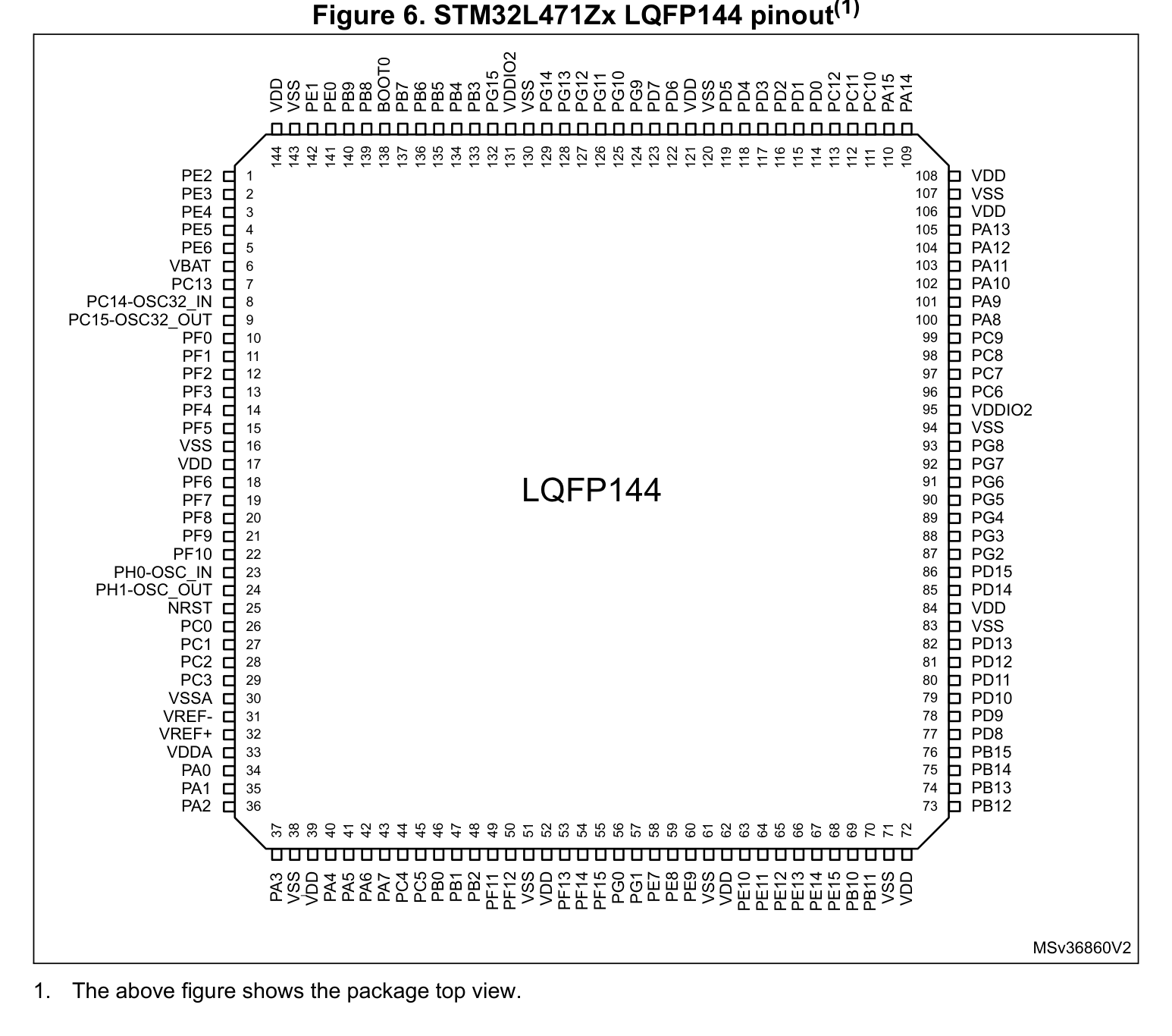
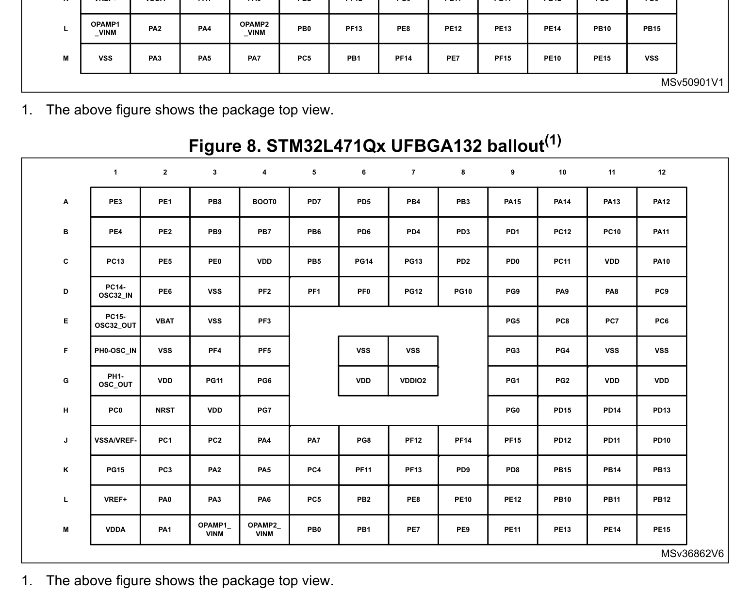
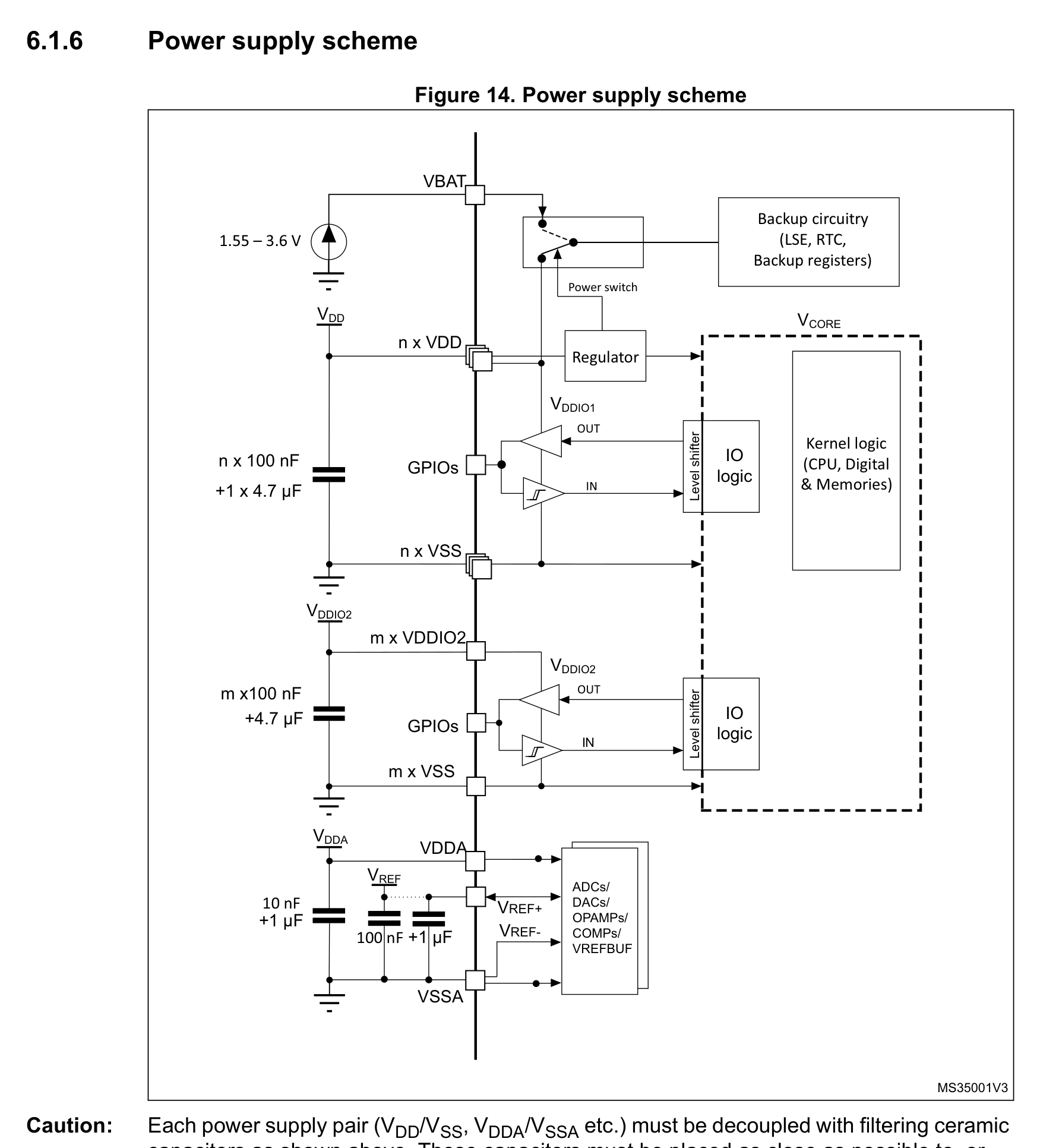
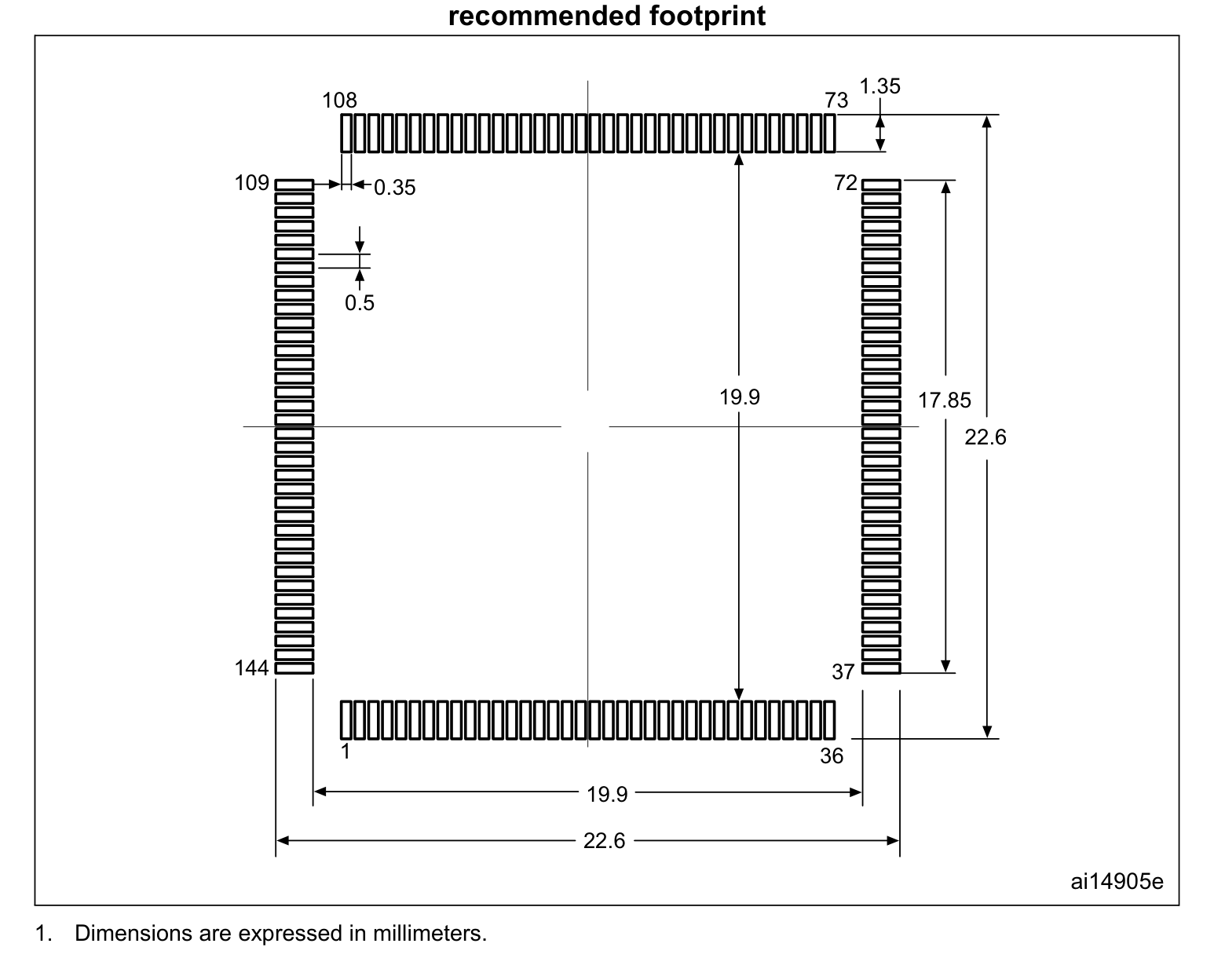
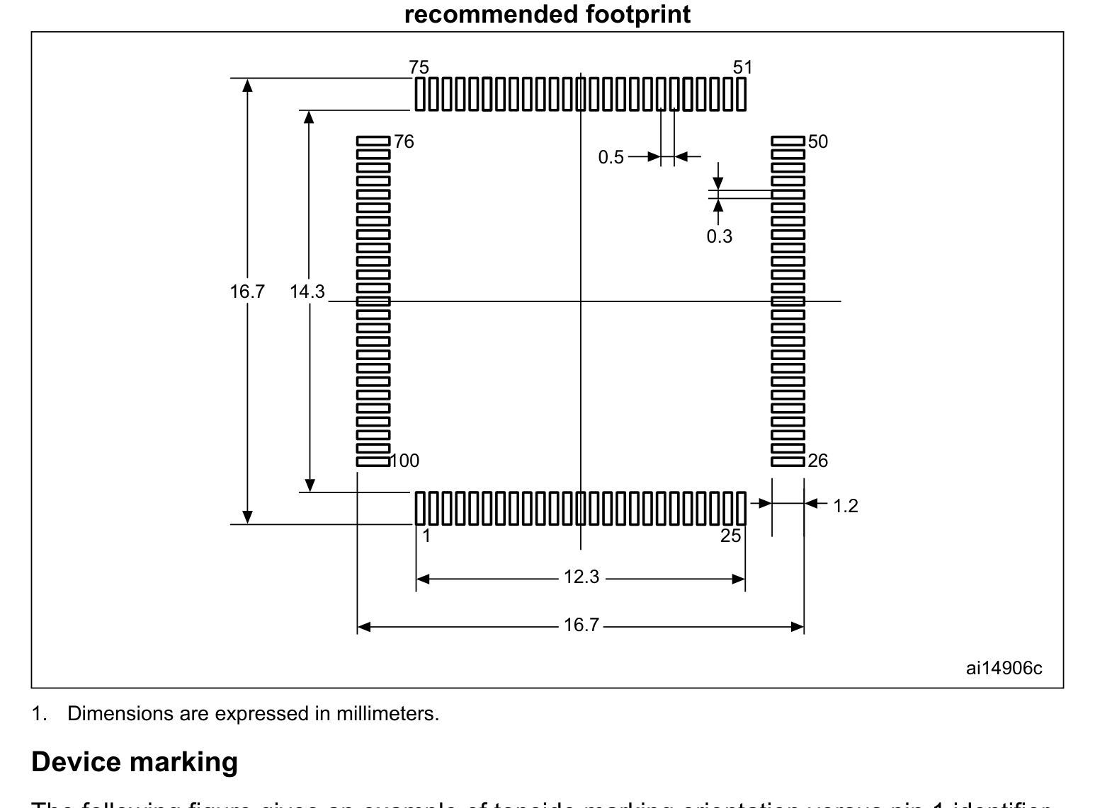
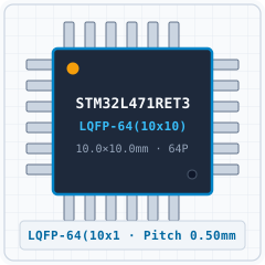
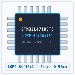
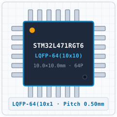
LQFP-64(10x10) · 64P
| Pin | Symbol | Typ | Funktionsbeschreibung (DE) |
|---|---|---|---|
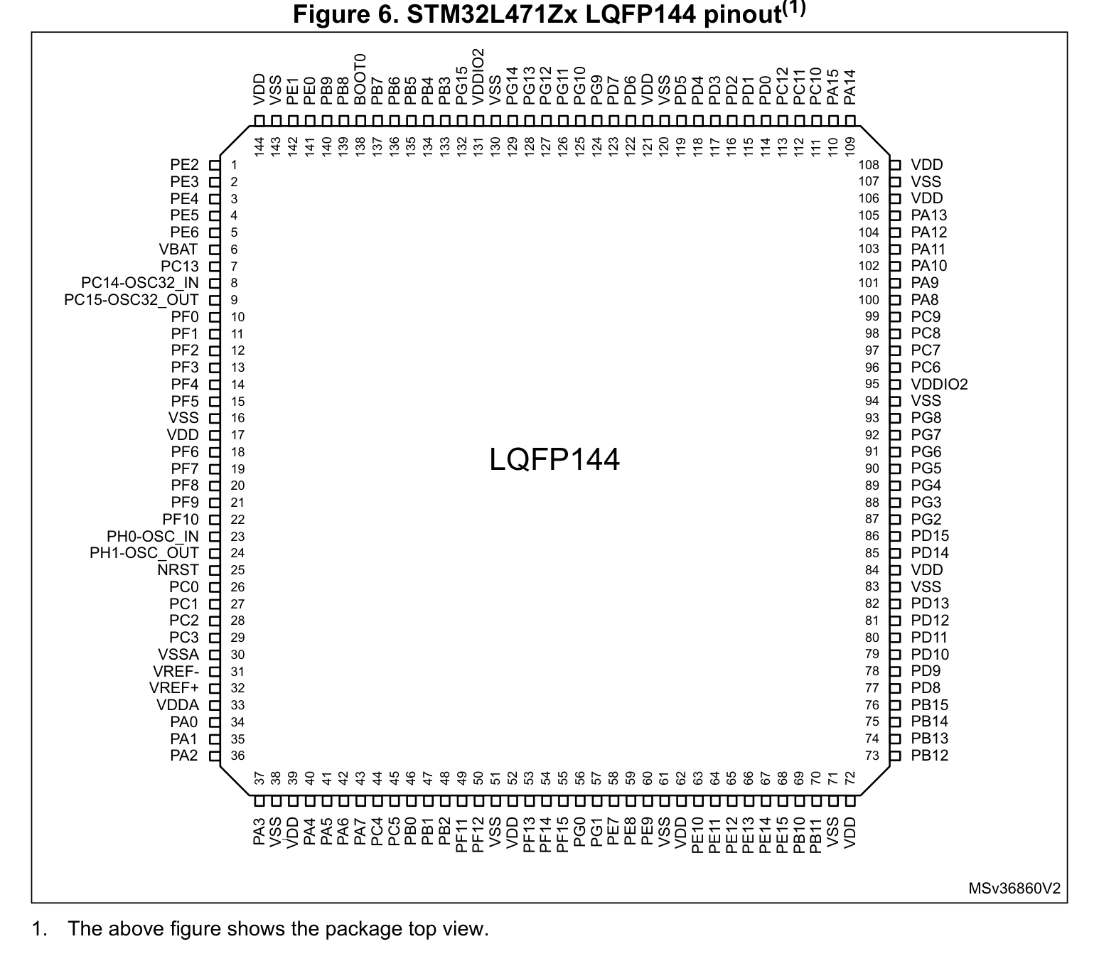
| 1 | PE2 | I/O | Multiplex-I/O- & Peripherie-Pin PE2 (General) |
| 2 | PE3 | I/O | Multiplex-I/O- & Peripherie-Pin PE3 (General) |
| 3 | PE4 | I/O | Multiplex-I/O- & Peripherie-Pin PE4 (General) |
| 4 | PE5 | I/O | Multiplex-I/O- & Peripherie-Pin PE5 (SPI) |
| 5 | PE6 | I/O | Multiplex-I/O- & Peripherie-Pin PE6 (RTC/CLK) |
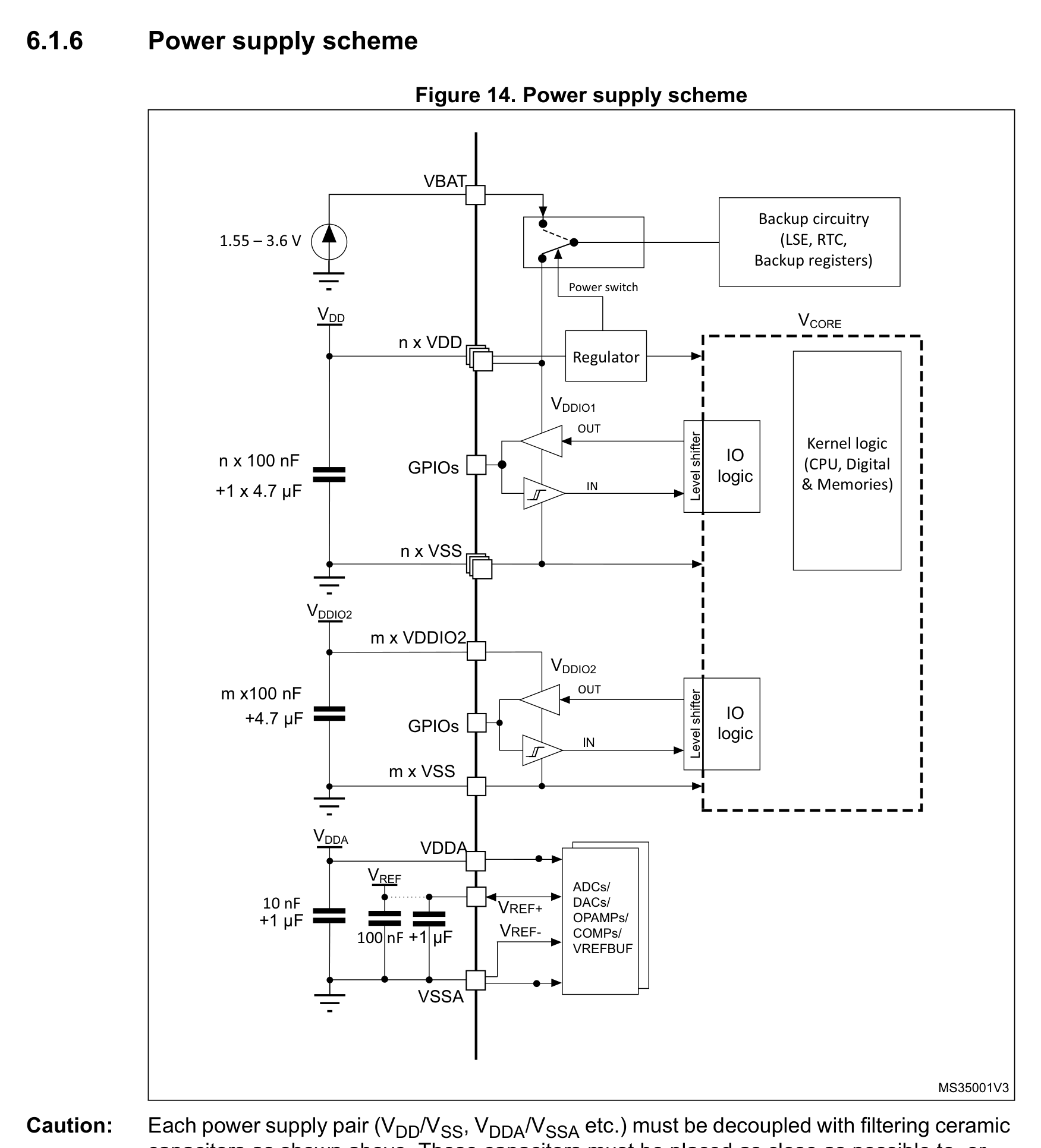
| 6 | VBAT | Power | Versorgungsspannungseingang (VBAT — 3.3V VDD (Max 4.0V)) |
| 7 | PC13 | I/O | Multiplex-I/O- & Peripherie-Pin PC13 (RTC/CLK) |
| 8 | PC14 - OSC32_IN (PC14) | I/O | Multiplex-I/O- & Peripherie-Pin PC14 - OSC32_IN (PC14) (RTC/CLK) |
| 9 | IO4 | I/O | GPIO4 / RTC_GPIO4 / TOUCH4 / ADC1_CH3 |
| 10 | PF0 | I/O | Multiplex-I/O- & Peripherie-Pin PF0 (I2C) |
| 11 | PF1 | I/O | Multiplex-I/O- & Peripherie-Pin PF1 (I2C) |
| 12 | PF2 | I/O | Multiplex-I/O- & Peripherie-Pin PF2 (I2C) |
| 13 | PF3 | I/O | Multiplex-I/O- & Peripherie-Pin PF3 (ADC) |
| 14 | PF4 | I/O | Multiplex-I/O- & Peripherie-Pin PF4 (ADC) |
| 15 | PF5 | I/O | Multiplex-I/O- & Peripherie-Pin PF5 (ADC) |
| 16 | VSS | GND | Masseanschluss (VSS) |
| 17 | VDD | Power | Versorgungsspannungseingang (VDD — 3.3V VDD (Max 4.0V)) |
| 18 | PF6 | I/O | Multiplex-I/O- & Peripherie-Pin PF6 (ADC) |
| 19 | PF7 | I/O | Multiplex-I/O- & Peripherie-Pin PF7 (ADC, PWM) |
| 20 | PF8 | I/O | Multiplex-I/O- & Peripherie-Pin PF8 (ADC) |
| 21 | PF9 | I/O | Multiplex-I/O- & Peripherie-Pin PF9 (ADC) |
| 22 | PF10 | I/O | Multiplex-I/O- & Peripherie-Pin PF10 (ADC) |
| 23 | PH0OSC IN -_ (PH0) | I/O | Multiplex-I/O- & Peripherie-Pin PH0OSC IN -_ (PH0) (RTC/CLK) |
| 24 | PH1OSC OUT -_ (PH1) | I/O | Multiplex-I/O- & Peripherie-Pin PH1OSC OUT -_ (PH1) (RTC/CLK) |
| 25 | NRST | I | Systemfreigabe & Hardware-Reset (NRST) |
| 26 | PC0 | I/O | Multiplex-I/O- & Peripherie-Pin PC0 (ADC) |
| 27 | PC1 | I/O | Multiplex-I/O- & Peripherie-Pin PC1 (ADC) |
| 28 | PC2 | I/O | Multiplex-I/O- & Peripherie-Pin PC2 (ADC) |
| 29 | PC3 | I/O | Multiplex-I/O- & Peripherie-Pin PC3 (I2C, ADC) |
| 30 | VSSA | GND | Masseanschluss (VSSA) |
| 31 | VREF - | Analog | Multiplex-I/O- & Peripherie-Pin VREF - (General) |
| 32 | VREF+ | Analog | Multiplex-I/O- & Peripherie-Pin VREF+ (General) |
| 33 | VDDA | Power | Versorgungsspannungseingang (VDDA — 3.3V VDD (Max 4.0V)) |
| 34 | PA0 | I/O | Multiplex-I/O- & Peripherie-Pin PA0 (UART, ADC, PWM, RTC/CLK) |
| 35 | PA1 | I/O | Multiplex-I/O- & Peripherie-Pin PA1 (UART, ADC, PWM) |
| 36 | PA2 | I/O | Multiplex-I/O- & Peripherie-Pin PA2 (UART, ADC, PWM) |
| 37 | PA3 | I/O | Multiplex-I/O- & Peripherie-Pin PA3 (UART, ADC, PWM) |
| 38 | VSS | GND | Masseanschluss (VSS) |
| 39 | VDD | Power | Versorgungsspannungseingang (VDD — 3.3V VDD (Max 4.0V)) |
| 40 | PA4 | I/O | Multiplex-I/O- & Peripherie-Pin PA4 (UART, SPI, ADC, DAC) |
| 41 | PA5 | I/O | Multiplex-I/O- & Peripherie-Pin PA5 (ADC, DAC, PWM) |
| 42 | PA6 | I/O | Multiplex-I/O- & Peripherie-Pin PA6 (UART, ADC) |
| 43 | PA7 | I/O | Multiplex-I/O- & Peripherie-Pin PA7 (ADC, PWM) |
| 44 | PC4 | I/O | Multiplex-I/O- & Peripherie-Pin PC4 (UART, ADC) |
| 45 | PC5 | I/O | Multiplex-I/O- & Peripherie-Pin PC5 (UART, ADC) |
| 46 | PB0 | I/O | Multiplex-I/O- & Peripherie-Pin PB0 (UART, ADC, PWM) |
| 47 | PB1 | I/O | Multiplex-I/O- & Peripherie-Pin PB1 (UART, ADC, PWM) |
| 48 | PB2 | I/O | Multiplex-I/O- & Peripherie-Pin PB2 (I2C, RTC/CLK) |
| 49 | PF11 | I/O | Multiplex-I/O- & Peripherie-Pin PF11 (General) |
| 50 | PF12 | I/O | Multiplex-I/O- & Peripherie-Pin PF12 (General) |
| 51 | VSS | GND | Masseanschluss (VSS) |
| 52 | VDD | Power | Versorgungsspannungseingang (VDD — 3.3V VDD (Max 4.0V)) |
| 53 | PF13 | I/O | Multiplex-I/O- & Peripherie-Pin PF13 (General) |
| 54 | PF14 | I/O | Multiplex-I/O- & Peripherie-Pin PF14 (General) |
| 55 | PF15 | I/O | Multiplex-I/O- & Peripherie-Pin PF15 (General) |
| 56 | PG0 | I/O | Multiplex-I/O- & Peripherie-Pin PG0 (General) |
| 57 | PG1 | I/O | Multiplex-I/O- & Peripherie-Pin PG1 (General) |
| 58 | PE7 | I/O | Multiplex-I/O- & Peripherie-Pin PE7 (General) |
| 59 | PE8 | I/O | Multiplex-I/O- & Peripherie-Pin PE8 (PWM) |
| 60 | PE9 | I/O | Multiplex-I/O- & Peripherie-Pin PE9 (PWM) |
| 61 | VSS | GND | Masseanschluss (VSS) |
| 62 | VDD | Power | Versorgungsspannungseingang (VDD — 3.3V VDD (Max 4.0V)) |
| 63 | PE10 | I/O | Multiplex-I/O- & Peripherie-Pin PE10 (PWM) |
| 64 | PE11 | I/O | Multiplex-I/O- & Peripherie-Pin PE11 (PWM) |
| 65 | PE12 | I/O | Multiplex-I/O- & Peripherie-Pin PE12 (PWM) |
| 66 | PE13 | I/O | Multiplex-I/O- & Peripherie-Pin PE13 (PWM) |
| 67 | PE14 | I/O | Multiplex-I/O- & Peripherie-Pin PE14 (SPI, PWM) |
| 68 | PE15 | I/O | Multiplex-I/O- & Peripherie-Pin PE15 (SPI) |
| 69 | PB10 | I/O | Multiplex-I/O- & Peripherie-Pin PB10 (UART, SPI, PWM) |
| 70 | PB11 | I/O | Multiplex-I/O- & Peripherie-Pin PB11 (UART, PWM) |
| 71 | VSS | GND | Masseanschluss (VSS) |
| 72 | VDD | Power | Versorgungsspannungseingang (VDD — 3.3V VDD (Max 4.0V)) |
| 73 | PB12 | I/O | Multiplex-I/O- & Peripherie-Pin PB12 (UART, I2C) |
| 74 | PB13 | I/O | Multiplex-I/O- & Peripherie-Pin PB13 (UART, SPI, PWM) |
| 75 | PB14 | I/O | Multiplex-I/O- & Peripherie-Pin PB14 (UART, I2C, PWM) |
| 76 | PB15 | I/O | Multiplex-I/O- & Peripherie-Pin PB15 (PWM, RTC/CLK) |
| 77 | PD8 | I/O | Multiplex-I/O- & Peripherie-Pin PD8 (UART) |
| 78 | PD9 | I/O | Multiplex-I/O- & Peripherie-Pin PD9 (UART) |
| 79 | PD10 | I/O | Multiplex-I/O- & Peripherie-Pin PD10 (UART, SPI) |
| 80 | PD11 | I/O | Multiplex-I/O- & Peripherie-Pin PD11 (UART, I2C) |
| 81 | PD12 | I/O | Multiplex-I/O- & Peripherie-Pin PD12 (UART, PWM) |
| 82 | PD13 | I/O | Multiplex-I/O- & Peripherie-Pin PD13 (General) |
| 83 | VSS | GND | Masseanschluss (VSS) |
| 84 | VDD | Power | Versorgungsspannungseingang (VDD — 3.3V VDD (Max 4.0V)) |
| 85 | PD14 | I/O | Multiplex-I/O- & Peripherie-Pin PD14 (PWM) |
| 86 | PD15 | I/O | Multiplex-I/O- & Peripherie-Pin PD15 (PWM) |
| 87 | PG2 | I/O | Multiplex-I/O- & Peripherie-Pin PG2 (SPI) |
| 88 | PG3 | I/O | Multiplex-I/O- & Peripherie-Pin PG3 (SPI) |
| 89 | PG4 | I/O | Multiplex-I/O- & Peripherie-Pin PG4 (SPI) |
| 90 | PG5 | I/O | Multiplex-I/O- & Peripherie-Pin PG5 (UART, SPI) |
| 91 | PG6 | I/O | Multiplex-I/O- & Peripherie-Pin PG6 (UART, I2C) |
| 92 | PG7 | I/O | Multiplex-I/O- & Peripherie-Pin PG7 (I2C) |
| 93 | PG8 | I/O | Multiplex-I/O- & Peripherie-Pin PG8 (I2C) |
| 94 | VSS | GND | Masseanschluss (VSS) |
| 95 | VDDIO2 | Power | Versorgungsspannungseingang (VDDIO2 — 3.3V VDD (Max 4.0V)) |
| 96 | PC6 | I/O | Multiplex-I/O- & Peripherie-Pin PC6 (PWM) |
| 97 | PC7 | I/O | Multiplex-I/O- & Peripherie-Pin PC7 (PWM) |
| 98 | PC8 | I/O | Multiplex-I/O- & Peripherie-Pin PC8 (PWM) |
| 99 | PC9 | I/O | Multiplex-I/O- & Peripherie-Pin PC9 (General) |
| 100 | PA8 | I/O | Multiplex-I/O- & Peripherie-Pin PA8 (UART, RTC/CLK) |
| 101 | PA9 | I/O | Multiplex-I/O- & Peripherie-Pin PA9 (PWM) |
| 102 | PA10 | I/O | Multiplex-I/O- & Peripherie-Pin PA10 (PWM) |
| 103 | PA11 | I/O | Multiplex-I/O- & Peripherie-Pin PA11 (UART, PWM) |
| 104 | PA12 | I/O | Multiplex-I/O- & Peripherie-Pin PA12 (UART, CAN) |
| 105 | PA13 (JTMSSWDIO) - | I/O | Multiplex-I/O- & Peripherie-Pin PA13 (JTMSSWDIO) - (SWD/JTAG) |
| 106 | VDD | Power | Versorgungsspannungseingang (VDD — 3.3V VDD (Max 4.0V)) |
| 107 | VSS | GND | Masseanschluss (VSS) |
| 108 | VDD | Power | Versorgungsspannungseingang (VDD — 3.3V VDD (Max 4.0V)) |
| 109 | PA14 (JTCKSWCLK) - | I/O | Multiplex-I/O- & Peripherie-Pin PA14 (JTCKSWCLK) - (SWD/JTAG) |
| 110 | PA15(JTDI) | I/O | Multiplex-I/O- & Peripherie-Pin PA15(JTDI) (UART, SPI, SWD/JTAG) |
| 111 | PC10 | I/O | Multiplex-I/O- & Peripherie-Pin PC10 (UART, SPI) |
| 112 | PC11 | I/O | Multiplex-I/O- & Peripherie-Pin PC11 (UART, SPI) |
| 113 | PC12 | I/O | Multiplex-I/O- & Peripherie-Pin PC12 (UART, SPI) |
| 114 | PD0 | I/O | Multiplex-I/O- & Peripherie-Pin PD0 (SPI, CAN) |
| 115 | PD1 | I/O | Multiplex-I/O- & Peripherie-Pin PD1 (SPI, CAN) |
| 116 | PD2 | I/O | Multiplex-I/O- & Peripherie-Pin PD2 (UART) |
| 117 | PD3 | I/O | Multiplex-I/O- & Peripherie-Pin PD3 (UART, SPI) |
| 118 | PD4 | I/O | Multiplex-I/O- & Peripherie-Pin PD4 (UART, SPI) |
| 119 | PD5 | I/O | Multiplex-I/O- & Peripherie-Pin PD5 (UART) |
| 120 | VSS | GND | Masseanschluss (VSS) |
| 121 | VDD | Power | Versorgungsspannungseingang (VDD — 3.3V VDD (Max 4.0V)) |
| 122 | PD6 | I/O | Multiplex-I/O- & Peripherie-Pin PD6 (UART) |
| 123 | PD7 | I/O | Multiplex-I/O- & Peripherie-Pin PD7 (UART) |
| 124 | PG9 | I/O | Multiplex-I/O- & Peripherie-Pin PG9 (SPI) |
| 125 | PG10 | I/O | Multiplex-I/O- & Peripherie-Pin PG10 (UART) |
| 126 | PG11 | I/O | Multiplex-I/O- & Peripherie-Pin PG11 (UART) |
| 127 | PG12 | I/O | Multiplex-I/O- & Peripherie-Pin PG12 (UART) |
| 128 | PG13 | I/O | Multiplex-I/O- & Peripherie-Pin PG13 (I2C) |
| 129 | PG14 | I/O | Multiplex-I/O- & Peripherie-Pin PG14 (I2C) |
| 130 | VSS | GND | Masseanschluss (VSS) |
| 131 | VDDIO2 | Power | Versorgungsspannungseingang (VDDIO2 — 3.3V VDD (Max 4.0V)) |
| 132 | PG15 | I/O | Multiplex-I/O- & Peripherie-Pin PG15 (I2C) |
| 133 | PB3 (JTDO - TRACESWO) | I/O | Multiplex-I/O- & Peripherie-Pin PB3 (JTDO - TRACESWO) (UART, SPI, PWM, SWD/JTAG) |
| 134 | PB4 (NJTRST) | I/O | Multiplex-I/O- & Peripherie-Pin PB4 (NJTRST) (UART, SPI, SWD/JTAG) |
| 135 | PB5 | I/O | Multiplex-I/O- & Peripherie-Pin PB5 (UART, SPI, I2C) |
| 136 | PB6 | I/O | Multiplex-I/O- & Peripherie-Pin PB6 (UART) |
| 137 | PB7 | I/O | Multiplex-I/O- & Peripherie-Pin PB7 (UART) |
| 138 | BOOT0 | I | Reiner Eingangs-Pin BOOT0 (General) |
| 139 | PB8 | I/O | Multiplex-I/O- & Peripherie-Pin PB8 (PWM, CAN) |
| 140 | PB9 | I/O | Multiplex-I/O- & Peripherie-Pin PB9 (I2C, CAN) |
| 141 | PE0 | I/O | Multiplex-I/O- & Peripherie-Pin PE0 (General) |
| 142 | PE1 | I/O | Multiplex-I/O- & Peripherie-Pin PE1 (General) |
| 143 | VSS | GND | Masseanschluss (VSS) |
| 144 | VDD | Power | Versorgungsspannungseingang (VDD — 3.3V VDD (Max 4.0V)) |
| Bauteilbezeichner / Ersatz-MPN | Wert / Gehäuse | Funktion & PCB-Layout-Regel |
|---|---|---|
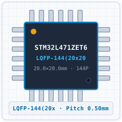
| N/A BOM | Per application circuit LQFP-144(20x20) | Leiterbahnbreiten für Nennstrom dimensionieren und IPC-2221 Isolationsabstände einhalten. |
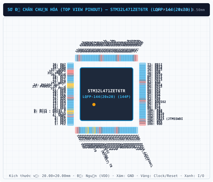
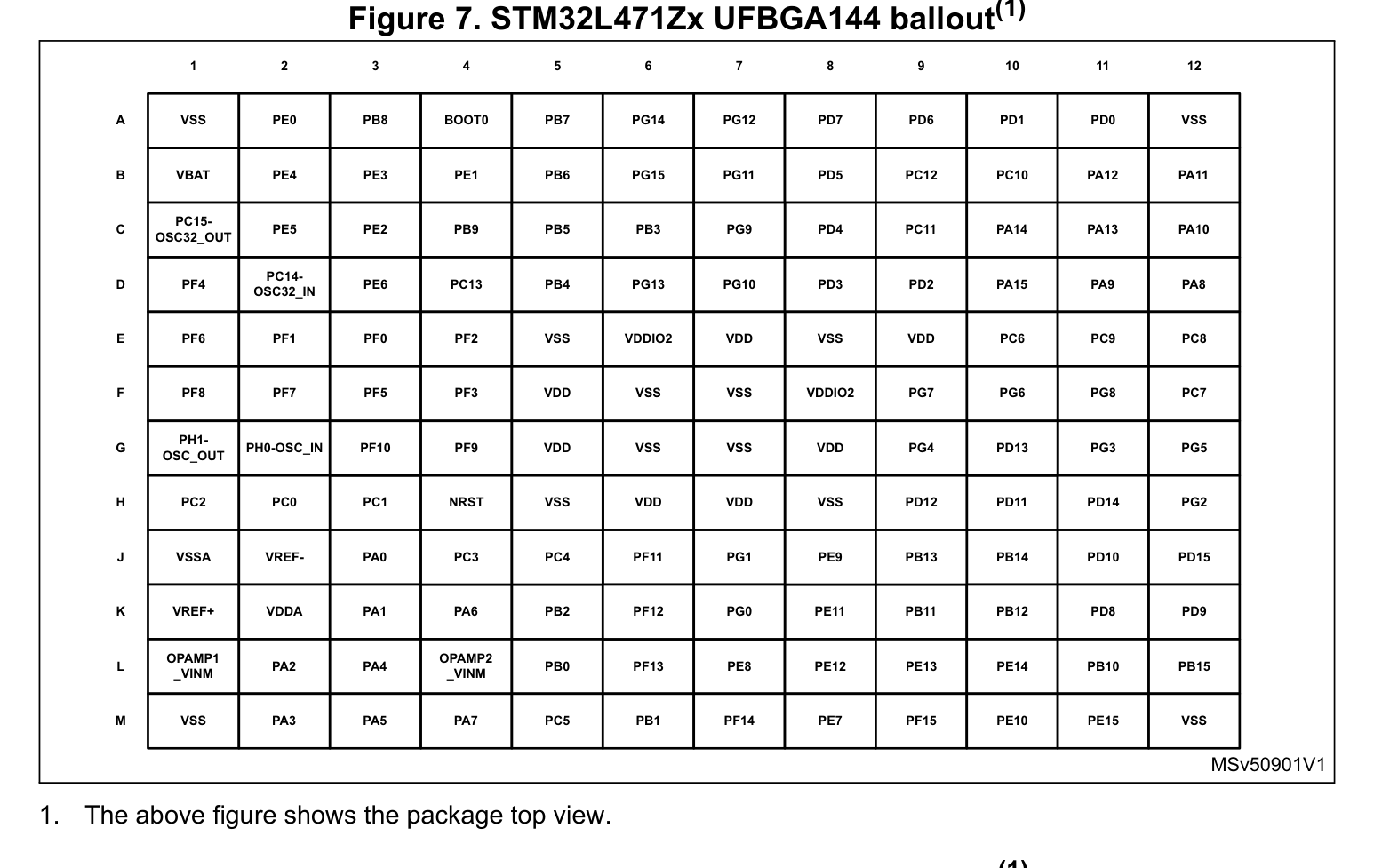
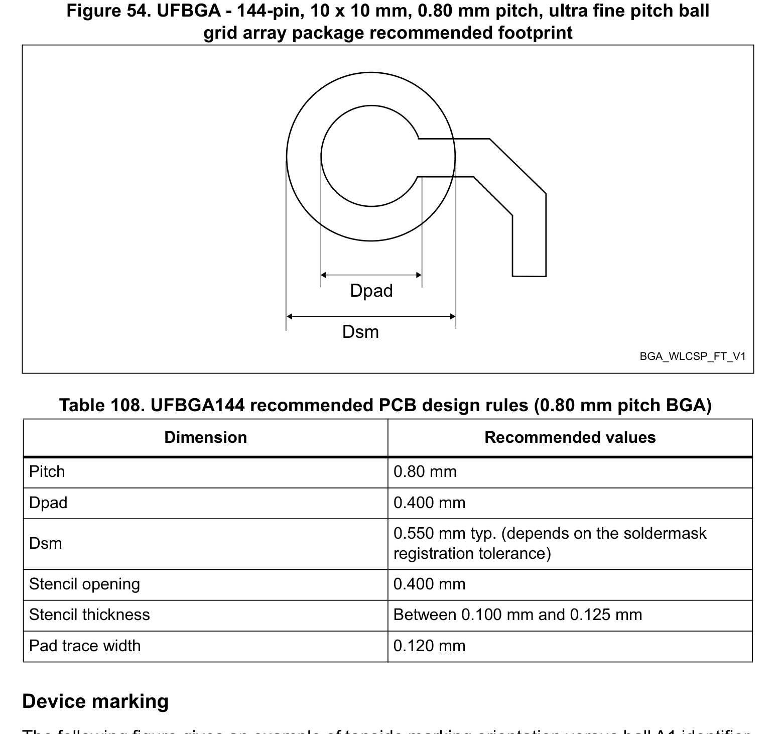
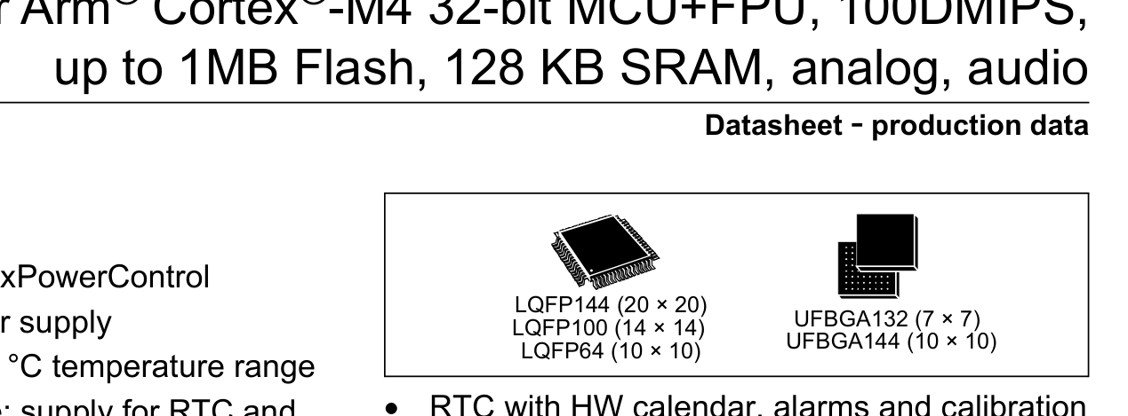
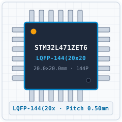
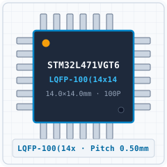
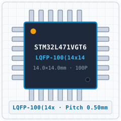
Das Bauteil STM32L471ZET6TR von ST im LQFP-144(20x20)-Gehäuse besitzt 144 Pins mit einem Rastermaß (Pitch) von 0.50 mm und einem Betriebsspannungsbereich VCC von 1.71 V to 3.6 V. Wichtige Pins: 1 (PE2: Multiplex-I/O- & Peripherie-Pin PE2 (General)), 2 (PE3: Multiplex-I/O- & Peripherie-Pin PE3 (General)), 3 (PE4: Multiplex-I/O- & Peripherie-Pin PE4 (General)), 4 (PE5: Multiplex-I/O- & Peripherie-Pin PE5 (SPI)), 5 (PE6: Multiplex-I/O- & Peripherie-Pin PE6 (RTC/CLK)), 6 (VBAT: Versorgungsspannungseingang (VBAT — 3.3V VDD (Max 4.0V))).
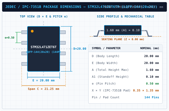
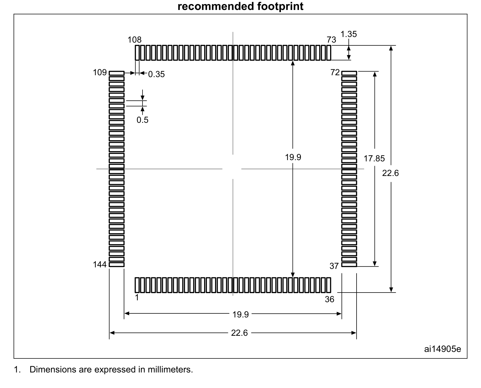
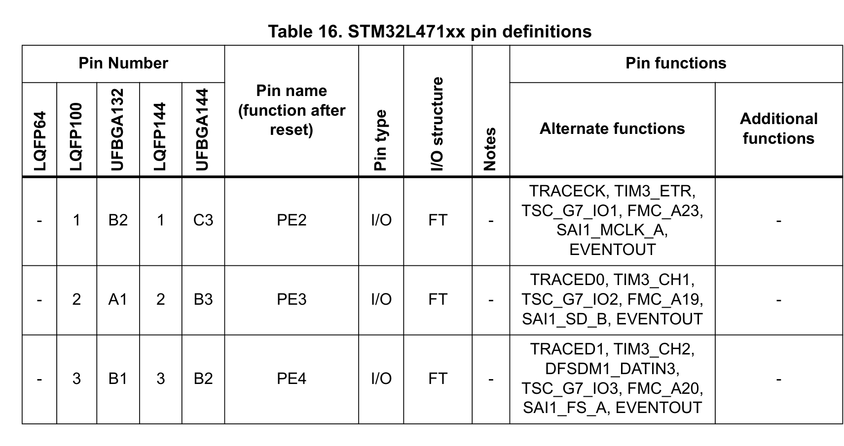
Gemäß Datenblatt und IPC-7351B (Density Level B Nominal) betragen die Gehäusemaße des STM32L471ZET6TR (LQFP-144(20x20)) 20.00 × 20.00 mm bei einem Pitch e = 0.50 mm und 144 Kupfer-Pads.
Auf dieser Seite können Sie das vollständig verifizierte CAD-Bibliothekspaket für STM32L471ZET6TR (ST, LQFP-144(20x20)) unter der Open-Hardware-Lizenz CERN-OHL-P-2.0 kostenlos herunterladen: KiCad 8 Footprint (.kicad_mod), Schaltplansymbol (.kicad_sym), Fusion 360 / Eagle (.lbr) und 3D STEP AP214 / WebGL GLB.
| Pin-Nr. | Signalname | Elektrischer Typ | Funktionsbeschreibung & Schaltungshinweise |
|---|---|---|---|
| 1 | PE2 | Digital_IO | Signalanschluss PE2 (Richtung: I/O, Spannungsbereich: 3.3V VDD (Max 4.0V)). Alternative Multiplex-Funktionen: PE2. Unterstützte Bus-Schnittstellen: General. |
| 2 | PE3 | Digital_IO | Signalanschluss PE3 (Richtung: I/O, Spannungsbereich: 3.3V VDD (Max 4.0V)). Alternative Multiplex-Funktionen: PE3. Unterstützte Bus-Schnittstellen: General. |
| 3 | PE4 | Digital_IO | Signalanschluss PE4 (Richtung: I/O, Spannungsbereich: 3.3V VDD (Max 4.0V)). Alternative Multiplex-Funktionen: PE4. Unterstützte Bus-Schnittstellen: General. |
| 4 | PE5 | Digital_IO | Signalanschluss PE5 (Richtung: I/O, Spannungsbereich: 3.3V VDD (5V-Tolerant FT)). Alternative Multiplex-Funktionen: PE5. Unterstützte Bus-Schnittstellen: SPI. |
| 5 | PE6 | Digital_IO | Signalanschluss PE6 (Richtung: I/O, Spannungsbereich: 3.3V VDD (5V-Tolerant FT)). Alternative Multiplex-Funktionen: PE6. Unterstützte Bus-Schnittstellen: RTC/CLK. |
| 6 | VBAT | Power_In | Positiver Versorgungseingang (VBAT) im Spannungsbereich 3.3V VDD (Max 4.0V) (Max. 4.0V). |
| 7 | PC13 | Digital_IO | Signalanschluss PC13 (Richtung: I/O, Spannungsbereich: 3.3V VDD (5V-Tolerant FT)). Alternative Multiplex-Funktionen: PC13. Unterstützte Bus-Schnittstellen: RTC/CLK. |
| 8 | PC14 - OSC32_IN (PC14) | Digital_IO | Signalanschluss PC14 - OSC32_IN (PC14) (Richtung: I/O, Spannungsbereich: 3.3V VDD (5V-Tolerant FT)). Alternative Multiplex-Funktionen: PC14 - OSC32_IN (PC14). Unterstützte Bus-Schnittstellen: RTC/CLK. |
| 9 | IO4 | Digital_IO | GPIO4 / RTC_GPIO4 / TOUCH4 / ADC1_CH3 |
| 10 | PF0 | Digital_IO | Signalanschluss PF0 (Richtung: I/O, Spannungsbereich: 3.3V VDD (5V-Tolerant FT)). Alternative Multiplex-Funktionen: PF0. Unterstützte Bus-Schnittstellen: I2C. |
| 11 | PF1 | Digital_IO | Signalanschluss PF1 (Richtung: I/O, Spannungsbereich: 3.3V VDD (5V-Tolerant FT)). Alternative Multiplex-Funktionen: PF1. Unterstützte Bus-Schnittstellen: I2C. |
| 12 | PF2 | Digital_IO | Signalanschluss PF2 (Richtung: I/O, Spannungsbereich: 3.3V VDD (5V-Tolerant FT)). Alternative Multiplex-Funktionen: PF2. Unterstützte Bus-Schnittstellen: I2C. |
| 13 | PF3 | Digital_IO | Signalanschluss PF3 (Richtung: I/O, Spannungsbereich: 3.3V VDD (5V-Tolerant FT)). Alternative Multiplex-Funktionen: PF3. Unterstützte Bus-Schnittstellen: ADC. |
| 14 | PF4 | Digital_IO | Signalanschluss PF4 (Richtung: I/O, Spannungsbereich: 3.3V VDD (5V-Tolerant FT)). Alternative Multiplex-Funktionen: PF4. Unterstützte Bus-Schnittstellen: ADC. |
| 15 | PF5 | Digital_IO | Signalanschluss PF5 (Richtung: I/O, Spannungsbereich: 3.3V VDD (5V-Tolerant FT)). Alternative Multiplex-Funktionen: PF5. Unterstützte Bus-Schnittstellen: ADC. |
| 16 | VSS | GND | Elektrischer 0V-Masserückführungsanschluss (VSS) für Kernlogik, I/O-Treiber und Analogblöcke. |
| 17 | VDD | Power_In | Positiver Versorgungseingang (VDD) im Spannungsbereich 3.3V VDD (Max 4.0V) (Max. 4.0V). |
| 18 | PF6 | Digital_IO | Signalanschluss PF6 (Richtung: I/O, Spannungsbereich: 3.3V VDD (5V-Tolerant FT)). Alternative Multiplex-Funktionen: PF6. Unterstützte Bus-Schnittstellen: ADC. |
| 19 | PF7 | Digital_IO | Signalanschluss PF7 (Richtung: I/O, Spannungsbereich: 3.3V VDD (5V-Tolerant FT)). Alternative Multiplex-Funktionen: PF7. Unterstützte Bus-Schnittstellen: ADC, PWM. |
| 20 | PF8 | Digital_IO | Signalanschluss PF8 (Richtung: I/O, Spannungsbereich: 3.3V VDD (5V-Tolerant FT)). Alternative Multiplex-Funktionen: PF8. Unterstützte Bus-Schnittstellen: ADC. |
| 21 | PF9 | Digital_IO | Signalanschluss PF9 (Richtung: I/O, Spannungsbereich: 3.3V VDD (5V-Tolerant FT)). Alternative Multiplex-Funktionen: PF9. Unterstützte Bus-Schnittstellen: ADC. |
| 22 | PF10 | Digital_IO | Signalanschluss PF10 (Richtung: I/O, Spannungsbereich: 3.3V VDD (5V-Tolerant FT)). Alternative Multiplex-Funktionen: PF10. Unterstützte Bus-Schnittstellen: ADC. |
| 23 | PH0OSC IN -_ (PH0) | Digital_IO | Signalanschluss PH0OSC IN -_ (PH0) (Richtung: I/O, Spannungsbereich: 3.3V VDD (5V-Tolerant FT)). Alternative Multiplex-Funktionen: PH0OSC IN -_ (PH0). Unterstützte Bus-Schnittstellen: RTC/CLK. |
| 24 | PH1OSC OUT -_ (PH1) | Digital_IO | Signalanschluss PH1OSC OUT -_ (PH1) (Richtung: I/O, Spannungsbereich: 3.3V VDD (5V-Tolerant FT)). Alternative Multiplex-Funktionen: PH1OSC OUT -_ (PH1). Unterstützte Bus-Schnittstellen: RTC/CLK. |
| 25 | NRST | Digital_IO | Aktiv-niedriger Hardware-Reset-Anschluss (NRST): Low-Pegel setzt Prozessorkern und Peripherie zurück. |
| 26 | PC0 | Digital_IO | Signalanschluss PC0 (Richtung: I/O, Spannungsbereich: 3.3V VDD (5V-Tolerant FT)). Alternative Multiplex-Funktionen: PC0. Unterstützte Bus-Schnittstellen: ADC. |
| 27 | PC1 | Digital_IO | Signalanschluss PC1 (Richtung: I/O, Spannungsbereich: 3.3V VDD (5V-Tolerant FT)). Alternative Multiplex-Funktionen: PC1. Unterstützte Bus-Schnittstellen: ADC. |
| 28 | PC2 | Digital_IO | Signalanschluss PC2 (Richtung: I/O, Spannungsbereich: 3.3V VDD (5V-Tolerant FT)). Alternative Multiplex-Funktionen: PC2. Unterstützte Bus-Schnittstellen: ADC. |
| 29 | PC3 | Digital_IO | Signalanschluss PC3 (Richtung: I/O, Spannungsbereich: 3.3V VDD (5V-Tolerant FT)). Alternative Multiplex-Funktionen: PC3. Unterstützte Bus-Schnittstellen: I2C, ADC. |
| 30 | VSSA | GND | Elektrischer 0V-Masserückführungsanschluss (VSSA) für Kernlogik, I/O-Treiber und Analogblöcke. |
| 31 | VREF - | Analog | Signalanschluss VREF - (Richtung: Analog, Spannungsbereich: 3.3V VDD (Max 4.0V)). Alternative Multiplex-Funktionen: VREF -. Unterstützte Bus-Schnittstellen: General. |
| 32 | VREF+ | Analog | Signalanschluss VREF+ (Richtung: Analog, Spannungsbereich: 3.3V VDD (Max 4.0V)). Alternative Multiplex-Funktionen: VREF+. Unterstützte Bus-Schnittstellen: General. |
| 33 | VDDA | Power_In | Positiver Versorgungseingang (VDDA) im Spannungsbereich 3.3V VDD (Max 4.0V) (Max. 4.0V). |
| 34 | PA0 | Digital_IO | Signalanschluss PA0 (Richtung: I/O, Spannungsbereich: 3.3V VDD (5V-Tolerant FT)). Alternative Multiplex-Funktionen: PA0. Unterstützte Bus-Schnittstellen: UART, ADC, PWM, RTC/CLK. |
| 35 | PA1 | Digital_IO | Signalanschluss PA1 (Richtung: I/O, Spannungsbereich: 3.3V VDD (5V-Tolerant FT)). Alternative Multiplex-Funktionen: PA1. Unterstützte Bus-Schnittstellen: UART, ADC, PWM. |
| 36 | PA2 | Digital_IO | Signalanschluss PA2 (Richtung: I/O, Spannungsbereich: 3.3V VDD (5V-Tolerant FT)). Alternative Multiplex-Funktionen: PA2. Unterstützte Bus-Schnittstellen: UART, ADC, PWM. |
| 37 | PA3 | Digital_IO | Signalanschluss PA3 (Richtung: I/O, Spannungsbereich: 3.3V VDD (Max 4.0V)). Alternative Multiplex-Funktionen: PA3. Unterstützte Bus-Schnittstellen: UART, ADC, PWM. |
| 38 | VSS | GND | Elektrischer 0V-Masserückführungsanschluss (VSS) für Kernlogik, I/O-Treiber und Analogblöcke. |
| 39 | VDD | Power_In | Positiver Versorgungseingang (VDD) im Spannungsbereich 3.3V VDD (Max 4.0V) (Max. 4.0V). |
| 40 | PA4 | Digital_IO | Signalanschluss PA4 (Richtung: I/O, Spannungsbereich: 3.3V VDD (Max 4.0V)). Alternative Multiplex-Funktionen: SPI1_NSSSPI3NSS. Unterstützte Bus-Schnittstellen: UART, SPI, ADC, DAC. |
| 41 | PA5 | Digital_IO | Signalanschluss PA5 (Richtung: I/O, Spannungsbereich: 3.3V VDD (Max 4.0V)). Alternative Multiplex-Funktionen: PA5. Unterstützte Bus-Schnittstellen: ADC, DAC, PWM. |
| 42 | PA6 | Digital_IO | Signalanschluss PA6 (Richtung: I/O, Spannungsbereich: 3.3V VDD (5V-Tolerant FT)). Alternative Multiplex-Funktionen: PA6. Unterstützte Bus-Schnittstellen: UART, ADC. |
| 43 | PA7 | Digital_IO | Signalanschluss PA7 (Richtung: I/O, Spannungsbereich: 3.3V VDD (5V-Tolerant FT)). Alternative Multiplex-Funktionen: PA7. Unterstützte Bus-Schnittstellen: ADC, PWM. |
| 44 | PC4 | Digital_IO | Signalanschluss PC4 (Richtung: I/O, Spannungsbereich: 3.3V VDD (5V-Tolerant FT)). Alternative Multiplex-Funktionen: PC4. Unterstützte Bus-Schnittstellen: UART, ADC. |
| 45 | PC5 | Digital_IO | Signalanschluss PC5 (Richtung: I/O, Spannungsbereich: 3.3V VDD (5V-Tolerant FT)). Alternative Multiplex-Funktionen: PC5. Unterstützte Bus-Schnittstellen: UART, ADC. |
| 46 | PB0 | Digital_IO | Signalanschluss PB0 (Richtung: I/O, Spannungsbereich: 3.3V VDD (Max 4.0V)). Alternative Multiplex-Funktionen: PB0. Unterstützte Bus-Schnittstellen: UART, ADC, PWM. |
| 47 | PB1 | Digital_IO | Signalanschluss PB1 (Richtung: I/O, Spannungsbereich: 3.3V VDD (5V-Tolerant FT)). Alternative Multiplex-Funktionen: PB1. Unterstützte Bus-Schnittstellen: UART, ADC, PWM. |
| 48 | PB2 | Digital_IO | Signalanschluss PB2 (Richtung: I/O, Spannungsbereich: 3.3V VDD (5V-Tolerant FT)). Alternative Multiplex-Funktionen: I2C3_SMBA. Unterstützte Bus-Schnittstellen: I2C, RTC/CLK. |
| 49 | PF11 | Digital_IO | Signalanschluss PF11 (Richtung: I/O, Spannungsbereich: 3.3V VDD (5V-Tolerant FT)). Alternative Multiplex-Funktionen: PF11. Unterstützte Bus-Schnittstellen: General. |
| 50 | PF12 | Digital_IO | Signalanschluss PF12 (Richtung: I/O, Spannungsbereich: 3.3V VDD (5V-Tolerant FT)). Alternative Multiplex-Funktionen: PF12. Unterstützte Bus-Schnittstellen: General. |
| 51 | VSS | GND | Elektrischer 0V-Masserückführungsanschluss (VSS) für Kernlogik, I/O-Treiber und Analogblöcke. |
| 52 | VDD | Power_In | Positiver Versorgungseingang (VDD) im Spannungsbereich 3.3V VDD (Max 4.0V) (Max. 4.0V). |
| 53 | PF13 | Digital_IO | Signalanschluss PF13 (Richtung: I/O, Spannungsbereich: 3.3V VDD (5V-Tolerant FT)). Alternative Multiplex-Funktionen: PF13. Unterstützte Bus-Schnittstellen: General. |
| 54 | PF14 | Digital_IO | Signalanschluss PF14 (Richtung: I/O, Spannungsbereich: 3.3V VDD (5V-Tolerant FT)). Alternative Multiplex-Funktionen: PF14. Unterstützte Bus-Schnittstellen: General. |
| 55 | PF15 | Digital_IO | Signalanschluss PF15 (Richtung: I/O, Spannungsbereich: 3.3V VDD (5V-Tolerant FT)). Alternative Multiplex-Funktionen: PF15. Unterstützte Bus-Schnittstellen: General. |
| 56 | PG0 | Digital_IO | Signalanschluss PG0 (Richtung: I/O, Spannungsbereich: 3.3V VDD (5V-Tolerant FT)). Alternative Multiplex-Funktionen: PG0. Unterstützte Bus-Schnittstellen: General. |
| 57 | PG1 | Digital_IO | Signalanschluss PG1 (Richtung: I/O, Spannungsbereich: 3.3V VDD (5V-Tolerant FT)). Alternative Multiplex-Funktionen: PG1. Unterstützte Bus-Schnittstellen: General. |
| 58 | PE7 | Digital_IO | Signalanschluss PE7 (Richtung: I/O, Spannungsbereich: 3.3V VDD (5V-Tolerant FT)). Alternative Multiplex-Funktionen: PE7. Unterstützte Bus-Schnittstellen: General. |
| 59 | PE8 | Digital_IO | Signalanschluss PE8 (Richtung: I/O, Spannungsbereich: 3.3V VDD (5V-Tolerant FT)). Alternative Multiplex-Funktionen: PE8. Unterstützte Bus-Schnittstellen: PWM. |
| 60 | PE9 | Digital_IO | Signalanschluss PE9 (Richtung: I/O, Spannungsbereich: 3.3V VDD (5V-Tolerant FT)). Alternative Multiplex-Funktionen: PE9. Unterstützte Bus-Schnittstellen: PWM. |
| 61 | VSS | GND | Elektrischer 0V-Masserückführungsanschluss (VSS) für Kernlogik, I/O-Treiber und Analogblöcke. |
| 62 | VDD | Power_In | Positiver Versorgungseingang (VDD) im Spannungsbereich 3.3V VDD (Max 4.0V) (Max. 4.0V). |
| 63 | PE10 | Digital_IO | Signalanschluss PE10 (Richtung: I/O, Spannungsbereich: 3.3V VDD (5V-Tolerant FT)). Alternative Multiplex-Funktionen: PE10. Unterstützte Bus-Schnittstellen: PWM. |
| 64 | PE11 | Digital_IO | Signalanschluss PE11 (Richtung: I/O, Spannungsbereich: 3.3V VDD (5V-Tolerant FT)). Alternative Multiplex-Funktionen: PE11. Unterstützte Bus-Schnittstellen: PWM. |